# A B C D E F G H I J K L M N O P Q R S T U V W X Y Z

Texas Instruments ADS1218 Data Sheet / Manual

Summary

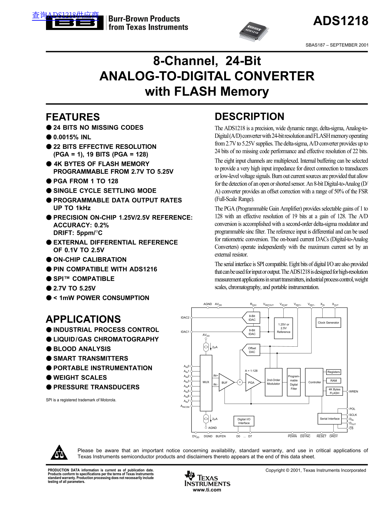
Achieve ultra-precise data acquisition with this 24-bit delta-sigma Analog-to-Digital Converter. Featuring wide dynamic range, internal flash memory, and high-resolution multiplexed channels, it is ideal for demanding instrumentation. The accompanying technical manual provides comprehensive details on setup, programmable gain (PGA), error correction, SPI interfacing, and specialized applications like industrial control, weight scales, and smart transmitters. This tool is essential for engineers and developers building portable or complex measurement systems requiring exceptional accuracy.
📄 Preview PAGE OF 30

Page 1 Text Content

查询ADS1218供应商

ADS1218

ADS1218

SBAS187 – SEPTEMBER 2001

8-Channel, 24-Bit

ANALOG-TO-DIGITAL CONVERTER with FLASH Memory

FEATURES DESCRIPTION

24 BITS NO MISSING CODES The ADS1218 is a precision, wide dynamic range, delta-sigma, Analog-to-

0.0015% INL Digital (A/D) converter with 24-bit resolution and FLASH memory operating from 2.7V to 5.25V supplies. The delta-sigma, A/D converter provides up to

22 BITS EFFECTIVE RESOLUTION

24 bits of no missing code performance and effective resolution of 22 bits.

(PGA = 1), 19 BITS (PGA = 128)

The eight input channels are multiplexed. Internal buffering can be selected

4K BYTES OF FLASH MEMORY

to provide a very high input impedance for direct connection to transducers

PROGRAMMABLE FROM 2.7V TO 5.25V

or low-level voltage signals. Burn out current sources are provided that allow

PGA FROM 1 TO 128

for the detection of an open or shorted sensor. An 8-bit Digital-to-Analog (D/

SINGLE CYCLE SETTLING MODE A) converter provides an offset correction with a range of 50% of the FSR

PROGRAMMABLE DATA OUTPUT RATES (Full-Scale Range).

UP TO 1k Hz The PGA (Programmable Gain Amplifier) provides selectable gains of 1 to

128 with an effective resolution of 19 bits at a gain of 128. The A/D

PRECISION ON-CHIP 1.25V/2.5V REFERENCE:

ACCURACY: 0.2% conversion is accomplished with a second-order delta-sigma modulator and DRIFT: 5ppm/°C programmable sinc filter. The reference input is differential and can be used for ratiometric conversion. The on-board current DACs (Digital-to-Analog

EXTERNAL DIFFERENTIAL REFERENCE

Converters) operate independently with the maximum current set by an

OF 0.1V TO 2.5V

external resistor.

ON-CHIP CALIBRATION

The serial interface is SPI compatible. Eight bits of digital I/O are also provided

PIN COMPATIBLE WITH ADS1216

that can be used for input or output. The ADS1218 is designed for high-resolution

SPI™ COMPATIBLE measurement applications in smart transmitters, industrial process control, weight

2.7V TO 5.25V scales, chromatography, and portable instrumentation.

< 1m W POWER CONSUMPTION

AGND AVDD RDAC VREFOUT VRCAP VREF+ VREF– XIN XOUT

8-Bit

IDAC2

APPLICATIONS IDAC

Clock Generator

1.25V or 2.5V

INDUSTRIAL PROCESS CONTROL 8-Bit

IDAC1 Reference

AVDD IDAC

LIQUID/GAS CHROMATOGRAPHY

2µA Offset

BLOOD ANALYSIS

SMART TRANSMITTERS

PORTABLE INSTRUMENTATION

AIN1 A = 1:128 Registers

AIN2 IN+ Program-

WEIGHT SCALES 2nd-Order

AIN3 mable RAM

MUX BUF PGA Controller

IN– Modulator Digital

PRESSURE TRANSDUCERS Filter 4K Bytes

AIN5 WREN

FLASH

SPI is a registered trademark of Motorola. AIN7

AINCOM

2µA Digital I/O Serial Interface DIN

Interface DOUT

AGND CS

D7...D0 DSYNCPDWN RESET DRDYBUFENDGNDDVDD

Please be aware that an important notice concerning availability, standard warranty, and use in critical applications of Texas Instruments semiconductor products and disclaimers thereto appears at the end of this data sheet.

PRODUCTION DATA information is current as of publication date. Copyright © 2001, Texas Instruments Incorporated Products conform to specifications per the terms of Texas Instruments standard warranty. Production processing does not necessarily include testing of all parameters.

www.ti.com

Page Summary Contents For Texas Instruments ADS1218 Data Sheet / Manual

Page 1 查询ADS1218供应商 ADS1218 ADS1218 SBAS187 – SEPTEMBER 2001 8-Channel, 24-Bit ANALOG-TO-DIGITAL CONVERTER with FLASH Memory FEATURES DESCRIPTION 24 BITS NO MISSING CODES The ADS1218 is a precision, wide dyn...
Page 2 ABSOLUTE MAXIMUM RATINGS(1) ELECTROSTATIC AVDD to AGND –0.3V to +6V DISCHARGE SENSITIVITY DVDD to DGND –0.3V to +6V Input Current 100m A, Momentary This integrated circuit can be damaged by ESD. Texas...
Page 3 ELECTRICAL CHARACTERISTICS: AVDD = 5V (Cont.) All specifications TMIN to TMAX, AVDD = +5V, DVDD = +2.7V to 5.25V, f MOD = 19.2k Hz, f OSC = 2.4576MHz, PGA = 1, Buffer ON, RDAC = 150kΩ, f DATA =10Hz, V...
Page 4 ELECTRICAL CHARACTERISTICS: AVDD = 3V All specifications TMIN to TMAX, AVDD = +3V, DVDD = +2.7V to 5.25V, f MOD = 19.2k Hz, f OSC = 2.4576MHz, PGA = 1, Buffer ON, RDAC = 75kΩ, f DATA=10Hz, VREF ≡ (REF...
Page 5 ELECTRICAL CHARACTERISTICS: AVDD = 3V (Cont.) All specifications TMIN to TMAX, AVDD = +3V, DVDD = +2.7V to 5.25V, f MOD = 19.2k Hz, f OSC = 2.4576MHz, PGA = 1, Buffer ON, RDAC = 75kΩ, f DATA=10Hz, VRE...
Page 6 PIN CONFIGURATION (TQFP-48) D0 RESET D1 BUFEN D2 DGND D3 DGND D4 DGND D5 DGND ADS1218 D6 WREN D7 RDAC AGND IDAC2 VREFOUT IDAC1 VREF+ VRCAP VREF– AVDD PIN DESCRIPTIONS PIN PIN NUMBER NAME DESCRIPTION N...
Page 7 TIMING SPECIFICATIONS SCLK (POL = 0) SCLK (POL = 1) DIN MSB LSB (Command or Command and Data) DOUT MSB(1) LSB(1) NOTE: (1) Bit Order = 0. ADS1218 SCLK Reset Waveform Resets On Falling Edge RESET, DSYN...
Page 8 TYPICAL CHARACTERISTICS AVDD = +5V, DVDD = +5V, f OSC = 2.4576MHz, PGA = 1, RDAC = 150kΩ, f DATA = 10Hz, VREF ≡ (REF IN+) – (REF IN–) = +2.5V, unless otherwise specified. rm s) rm s) rm s) EFFECTIVE N...
Page 9 TYPICAL CHARACTERISTICS (Cont.) AVDD = +5V, DVDD = +5V, f OSC = 2.4576MHz, PGA = 1, RDAC = 150kΩ, f DATA = 10Hz, VREF ≡ (REF IN+) – (REF IN–) = +2.5V, unless otherwise specified. ai (N or al iz ed d B...
Page 10 TYPICAL CHARACTERISTICS (Cont.) ur re nt µA ur re nt µA AVDD = +5V, DVDD = +5V, f OSC = 2.4576MHz, PGA = 1, RDAC = 150kΩ, f DATA = 10Hz, VREF ≡ (REF IN+) – (REF IN–) = +2.5V, unless otherwise specifie...
Page 11 TYPICAL CHARACTERISTICS (Cont.) AVDD = +5V, DVDD = +5V, f OSC = 2.4576MHz, PGA = 1, RDAC = 150kΩ, f DATA = 10Hz, VREF ≡ (REF IN+) – (REF IN–) = +2.5V, unless otherwise specified. or al iz ed ai or al ...
Page 12 OVERVIEW BURNOUT CURRENT SOURCES When the Burnout bit is set in the ACR configuration register, INPUT MULTIPLEXER two current sources are enabled. The current source on the The input multiplexer provi...
Page 13 CALIBRATION settling filter for the next two conversions, the first of which should be discarded. It will then use the sinc2 followed by the The offset and gain errors in the ADS1218, or the complete ...
Page 14 VOLTAGE REFERENCE DIGITAL I/O INTERFACE The voltage reference used for the ADS1218 can either be The ADS1218 has eight pins dedicated for digital I/O. The internal or external. The power-up configurat...
Page 15 MEMORY basis. Also, the RAM can be directly read or written through the serial interface on power-up. The banks allow separate Three types of memory are used on the ADS1218: registers, storage of sett...
Page 16 The RAM address space is linear, therefore accessing RAM The ADS1218 supports any combination of eight analog is done using an auto-incrementing pointer. Access to RAM inputs and the FLASH memory supp...
Page 17 DETAILED REGISTER DEFINITIONS ACR (Address 02H) Analog Control Register SETUP (Address 00H) Setup Register Reset Value = 00H Reset Value = iii01110 bit 7 bit 6 bit 5 bit 4 bit 3 bit 2 bit 1 bit 0 bit ...
Page 18 ODAC (Address 05H) Offset DAC Setting bit 5-4 SMODE1: SMODE0: Settling Mode Reset Value = 00H 00 = Auto (default) bit 7 bit 6 bit 5 bit 4 bit 3 bit 2 bit 1 bit 0 01 = Fast Settling filter 10 = Sinc2 f...
Page 19 COMMAND DEFINITIONS Operands: n = count (0 to 127) The commands listed below control the operation of the ADS1218. Some of the commands are stand-alone com- r = register (0 to 15) mands (e.g., RESET) ...
Page 20 STOPC Stop Continuous CREG Copy Registers to RAM Bank Description: Ends the continuous data output mode. Description: Copy the 16 control registers to the RAM bank Operands: None specified in the op c...
Page 21 WRAM Write to RAM CRAM Copy RAM Bank to Registers Description: Write up to 128 RAM locations starting at the Description: Copy the selected RAM Bank to the Configura- beginning of the RAM bank specifi...
Page 22 CSREG Calculate the Checksum of CSFL Calculate Checksum for all FLASH Pages Registers Description: Calculate the checksum for all FLASH pages. Description: Calculate the checksum of all the registers....
Page 23 SELFGCAL Gain Self Calibration DSYNC Sync DRDY Description: Starts the process of self-calibration for gain. Description: Synchronizes the ADS1218 to the serial clock The Full-Scale Register (FSR) is ...
Page 24 rdata rdatac stopc rreg rreg rreg rreg rreg rreg rreg rreg rreg rreg rreg rreg rreg rreg rreg rreg rram rram rram rram rram rram rram rram creg creg creg creg creg creg creg creg crega wreg wreg wreg ...
Page 25 SERIAL PERIPHERAL INTERFACE CS is used to select the device. It can be used to decode the ADS1218 in systems where a number of parts are connected The Serial Peripheral Interface (SPI), allows a contr...
Page 26 Effective Resolution—the effective resolution of the f SAMP—the frequency, or switching speed, of the input ADS1218 in a particular configuration can be expressed in sampling capacitor. The value is g...
Page 27 TOPIC INDEX TOPIC PAGE ABSOLUTE MAXIMUM RATINGS ..........................................................................................................................2 PACKAGE AND ORDERING INFORMA...
Page 28 PACKAGE DRAWING MTQF019A – JANUARY 1995 – REVISED JANUARY 1998 PFB (S-PQFP-G48) PLASTIC QUAD FLATPACK 0,13 NOM 5,50 TYP 7,20 SQ Gage Plane 6,80 9,20 SQ 8,80 0,25 0,05 MIN Seating Plane 0,45 1,20 MAX N...
Page 29 PACKAGE OPTION ADDENDUM www.ti.com 3-Oct-2003 PACKAGING INFORMATION ORDERABLE DEVICE STATUS(1) PACKAGE TYPE PACKAGE DRAWING PINS PACKAGE QTY ADS1218Y/250 ACTIVE TQFP PFB ADS1218Y/2K ACTIVE TQFP PFB (1...
Page 30 IMPORTANT NOTICE Texas Instruments Incorporated and its subsidiaries (TI) reserve the right to make corrections, modifications, enhancements, improvements, and other changes to its products and servic...

Manual Details

Brand Texas Instruments
Pages 30
File Size 463.01 KB
Published July 15, 2026
0 views

Enter the captcha to get the download link:

captcha

Frequently Asked Questions

What is the effective resolution of the ADS1218 converter?

It provides 24 bits of no missing code performance, with an effective resolution of up to 22 bits (PGA = 1).

How can I adjust the signal gain using the ADS1218?

The device features a Programmable Gain Amplifier (PGA) that allows selectable gains from 1 to 128.

What type of interface is used for data output and clocking?

The serial interface is SPI compatible, and eight bits of digital I/O are also provided.

What operating temperature range should the ADS1218 handle?

The recommended operating temperature range is –40°C to +85°C.