# A B C D E F G H I J K L M N O P Q R S T U V W X Y Z

Texas Instruments ADS1216 Data Sheet/Manual

Summary

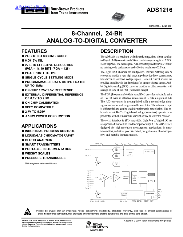
Texas Instruments ADS1216 8-channel 24-bit delta-sigma ADC data sheet for precision measurement. Features 24-bit resolution, PGA from 1 to 128, eight multiplexed inputs with high-impedance buffering, and on-chip 1.25V/2.5V reference. Covers SPI interface, data rates to 1kHz, offset DAC, burn-out detection, and calibration. For instrumentation engineers designing high-resolution measurement in industrial process control, chromatography, and portable instruments.
📄 Preview PAGE OF 28

Page 1 Text Content

查询ADS1216供应商

ADS1216

ADS1216

SBAS171B – JUNE 2001

8-Channel, 24-Bit

ANALOG-TO-DIGITAL CONVERTER

FEATURES DESCRIPTION 24 BITS NO MISSING CODES The ADS1216 is a precision, wide dynamic range, delta-sigma, Analog-

0.0015% INL to-Digital (A/D) converter with 24-bit resolution operating from 2.7V to 5.25V supplies. The delta-sigma, A/D converter provides up to 24 bits of

22 BITS EFFECTIVE RESOLUTION

no missing code performance and effective resolution of 22 bits.

(PGA = 1), 19 BITS (PGA = 128)

The eight input channels are multiplexed. Internal buffering can be

PGA FROM 1 TO 128

selected to provide a very high input impedance for direct connection to

SINGLE CYCLE SETTLING MODE

transducers or low-level voltage signals. Burn out current sources are

PROGRAMMABLE DATA OUTPUT RATES provided that allow for the detection of an open or shorted sensor. An 8- UP TO 1k Hz bit Digital-to-Analog (D/A) converter provides an offset correction with

ON-CHIP 1.25V/2.5V REFERENCE a range of 50% of the FSR (Full-Scale Range). EXTERNAL DIFFERENTIAL REFERENCE The PGA (Programmable Gain Amplifier) provides selectable gains OF 0.1V TO 2.5V of 1 to 128 with an effective resolution of 19 bits at a gain of 128. The A/D conversion is accomplished with a second-order delta-

ON-CHIP CALIBRATION

sigma modulator and programmable sinc filter. The reference input

SPI™ COMPATIBLE

is differential and can be used for ratiometric cancellation. The on-

2.7V TO 5.25V board current DACs (Digital-to-Analog Converters) operate inde-

< 1m W POWER CONSUMPTION pendently with the maximum current set by an external resistor. The serial interface is SPI compatible. Eight bits of digital I/O are also provided that can be used for input or output. The ADS1216 is

APPLICATIONS

designed for high-resolution measurement applications in smart

INDUSTRIAL PROCESS CONTROL transmitters, industrial process control, weight scales, chromatogra-

phy, and portable instrumentation.

LIQUID/GAS CHROMATOGRAPHY BLOOD ANALYSIS

AGND AVDD RDAC VREFOUT VRCAP VREF+ VREF– XIN XOUT

SMART TRANSMITTERS

PORTABLE INSTRUMENTATION 8-Bit

IDAC2

Clock Generator

1.25V or

WEIGHT SCALES 2.5V

8-Bit

IDAC1 Reference

AVDD IDAC

PRESSURE TRANSDUCERS

2µA Offset

SPI is a registered trademark of Motorola.

AIN1 A = 1:128

IN+ Registers

AIN2 Program-

AIN3 2nd-Order mable

MUX BUF PGA Controller

IN– Modulator Digital

Filter RAM

AIN5 AIN6 AIN7 AINCOM

2µA Digital I/O Serial Interface DIN

Interface DOUT

AGND CS

...D0 DSYNCPDWN RESET DRDYD7BUFENDGNDDVDD

Please be aware that an important notice concerning availability, standard warranty, and use in critical applications of Texas Instruments semiconductor products and disclaimers thereto appears at the end of this data sheet.

PRODUCTION DATA information is current as of publication date. Copyright © 2000, Texas Instruments Incorporated Products conform to specifications per the terms of Texas Instruments standard warranty. Production processing does not necessarily include testing of all parameters.

www.ti.com

Page Summary Contents For Texas Instruments ADS1216 Data Sheet/Manual

Page 1 查询ADS1216供应商 ADS1216 ADS1216 SBAS171B – JUNE 2001 8-Channel, 24-Bit ANALOG-TO-DIGITAL CONVERTER FEATURES DESCRIPTION 24 BITS NO MISSING CODES The ADS1216 is a precision, wide dynamic range, delta-sigm...
Page 2 ABSOLUTE MAXIMUM RATINGS(1) ELECTROSTATIC AVDD to AGND –0.3V to +6V DISCHARGE SENSITIVITY DVDD to DGND –0.3V to +6V Input Current 100m A, Momentary This integrated circuit can be damaged by ESD. Texas...
Page 3 ELECTRICAL CHARACTERISTICS: AVDD = 5V (Cont.) All specifications TMIN to TMAX, AVDD = +5V, DVDD = +2.7V to 5.25V, f MOD = 19.2k Hz, PGA = 1, Buffer ON, RDAC = 150kΩ, f DATA = 10Hz, VREF ≡ (REF IN+) – ...
Page 4 ELECTRICAL CHARACTERISTICS: AVDD = 3V All specifications TMIN to TMAX, AVDD = +3V, DVDD = +2.7V to 5.25V, f MOD = 19.2k Hz, PGA = 1, Buffer ON, RDAC = 75kΩ, f DATA = 10Hz, VREF ≡ (REF IN+) – (REF IN–)...
Page 5 ELECTRICAL CHARACTERISTICS: AVDD = 3V (Cont.) All specifications TMIN to TMAX, AVDD = +3V, DVDD = +2.7V to 5.25V, f MOD = 19.2k Hz, PGA = 1, Buffer ON, RDAC = 75kΩ, f DATA = 10Hz, VREF ≡ (REF IN+) – (...
Page 6 PIN CONFIGURATION Top View TQFP D0 RESET D1 BUFEN D2 DGND D3 DGND D4 DGND D5 DGND ADS1216 D6 DGND D7 RDAC AGND IDAC2 VREFOUT IDAC1 VREF+ VRCAP VREF– AVDD PIN DESCRIPTIONS PIN PIN NUMBER NAME DESCRIPTI...
Page 7 TIMING DIAGRAMS SCLK (POL = 0) SCLK (POL = 1) DIN MSB LSB (Command or Command and Data) DOUT MSB(1) LSB(1) NOTE: (1) Bit Order = 0. ADS1216 SCLK Reset Waveform Resets On Falling Edge RESET, DSYNC, PDW...
Page 8 TYPICAL CHARACTERISTICS AVDD = +5V, DVDD = +5V, f OSC = 2.4576MHz, PGA = 1, RDAC = 150kΩ, f DATA = 10Hz, VREF ≡ (REF IN+) – (REF IN–) = +2.5V, unless otherwise specified. rm s) rm s) rm s) EFFECTIVE N...
Page 9 TYPICAL CHARACTERISTICS (Cont.) AVDD = +5V, DVDD = +5V, f OSC = 2.4576MHz, PGA = 1, RDAC = 150kΩ, f DATA = 10Hz, VREF ≡ (REF IN+) – (REF IN–) = +2.5V, unless otherwise specified. ai (N or al iz ed d B...
Page 10 TYPICAL CHARACTERISTICS (Cont.) ur re nt µA ur re nt µA AVDD = +5V, DVDD = +5V, f OSC = 2.4576MHz, PGA = 1, RDAC = 150kΩ, f DATA = 10Hz, VREF ≡ (REF IN+) – (REF IN–) = +2.5V, unless otherwise specifie...
Page 11 TYPICAL CHARACTERISTICS (Cont.) AVDD = +5V, DVDD = +5V, f OSC = 2.4576MHz, PGA = 1, RDAC = 150kΩ, f DATA = 10Hz, VREF ≡ (REF IN+) – (REF IN–) = +2.5V, unless otherwise specified. or al iz ed ai or al ...
Page 12 OVERVIEW BURNOUT CURRENT SOURCES When the Burnout bit is set in the ACR configuration register, INPUT MULTIPLEXER two current sources are enabled. The current source on the The input multiplexer provi...
Page 13 CALIBRATION settling filter, for the next two conversions the first of which should be discarded. It will then use the sinc2 followed by the The offset and gain errors in the ADS1216, or the complete ...
Page 14 VOLTAGE REFERENCE as inputs or outputs. They are configured through the DIR control register. The DIR register defines whether the pin is an The voltage reference used for the ADS1216 can either be in...
Page 15 ADS1216 REGISTER BANK TOPOLOGY memory map, the address 0x14 is equivalent to bank 1 and offset 0x4. Simply stated, the most significant four bits The operation of the device is set up through individu...
Page 16 DETAILED REGISTER DEFINITIONS ACR (Address 02H) Analog Control Register SETUP (Address 00H) Setup Register Reset Value = 00H Reset Value = iii01110 bit 7 bit 6 bit 5 bit 4 bit 3 bit 2 bit 1 bit 0 bit ...
Page 17 ODAC (Address 05H) Offset DAC Setting U/B ANALOG INPUT DIGITAL OUTPUT Reset Value = 00H +FS 0x7FFFFF Zero 0x000000 bit 7 bit 6 bit 5 bit 4 bit 3 bit 2 bit 1 bit 0 –FS 0x800000 SIGN OSET6 OSET5 OSET4 O...
Page 18 ADS1216 CONTROL COMMAND DEFINITIONS The commands listed below control the operation of the Operands: ADS1216. Some of the commands are stand-alone com- n = count (0 to 127) mands (e.g., RESET) while o...
Page 19 STOPC Stop Continuous CREG Copy Registers to RAM Bank Description: Ends the continuous data output mode. Description: Copy the 16 control registers to the RAM bank Operands: None specified in the op c...
Page 20 WRAM Write to RAM CSARAMX Calculate the Checksum for all RAM Banks Description: Write up to 128 RAM locations starting at the beginning of the RAM bank specified as part of the instruc- Description: C...
Page 21 CSARAM Calculate Checksum for all SELFGCAL Gain Self Calibration RAM Banks Description: Starts the process of self-calibration for gain. Description: Calculate the checksum of all RAM Banks. The The F...
Page 22 DSYNC Sync DRDY RESET Reset to Powerup Values Description: Synchronizes the ADS1216 to the serial clock Description: Restore the registers to their power-up values. edge. This command will also stop t...
Page 23 SERIAL PERIPHERAL INTERFACE The timing specification shows the timing diagram for interfacing to the ADS1216 with CS used to decode the part. The Serial Peripheral Interface (SPI), allows a controller...
Page 24 Effective Resolution—the effective resolution of the f OSC—the frequency of the crystal oscillator or CMOS ADS1216 in a particular configuration can be expressed in compatible input signal at the XIN ...
Page 25 5V SUPPLY ANALOG INPUT(1) GENERAL EQUATIONS DIFFERENTIAL PGA OFFSET FULL-SCALE DIFFERENTIAL PGA SHIFT GAIN SETTING FULL-SCALE RANGE INPUT VOLTAGES(2) RANGE RANGE INPUT VOLTAGES(2) RANGE 5V ±2.5V ±1.25...
Page 26 TOPIC INDEX TOPIC PAGE ABSOLUTE MAXIMUM RATINGS ..........................................................................................................................2 PACKAGE/ORDERING INFORMATION...
Page 27 MECHANICAL DATA MTQF019A – JANUARY 1995 – REVISED JANUARY 1998 PFB (S-PQFP-G48) PLASTIC QUAD FLATPACK 0,13 NOM 5,50 TYP 7,20 SQ Gage Plane 6,80 9,20 SQ 8,80 0,25 0,05 MIN Seating Plane 0,45 1,20 MAX N...
Page 28 IMPORTANT NOTICE Texas Instruments Incorporated and its subsidiaries (TI) reserve the right to make corrections, modifications, enhancements, improvements, and other changes to its products and servic...

Manual Details

Brand Texas Instruments
Pages 28
File Size 448.16 KB
Published June 16, 2026
2 views

Enter the captcha to get the download link:

captcha

Frequently Asked Questions

What is the effective resolution at PGA gain 128?

19 bits effective resolution at PGA = 128.

What is the supply voltage range for the ADS1216?

Operates from 2.7V to 5.25V supplies.

How many input channels does the ADS1216 have?

It has eight multiplexed input channels.

What is the maximum programmable data output rate?

Programmable data output rates up to 1kHz.

Is the serial interface compatible with common protocols?

The serial interface is SPI compatible.