Texas Instruments ADS1206 ADS1207 Data Sheet Manual
Summary
These high-performance, low-cost Synchronous Voltage-to-Frequency Converters (VFC) include models ADS1206 and ADS1207. Designed for medium-resolution measurements, these devices convert input voltage into stable, synchronous frequency signals using external clock references. The product specification manual details operational parameters, including robust power supply flexibility (3.0V to 5.5V), low power consumption, and high effective resolution up to 12 bits. Ideal for engineers developing industrial control systems, motor drives, instrumentation, and portable measurement equipment requiring reliable signal conversion.
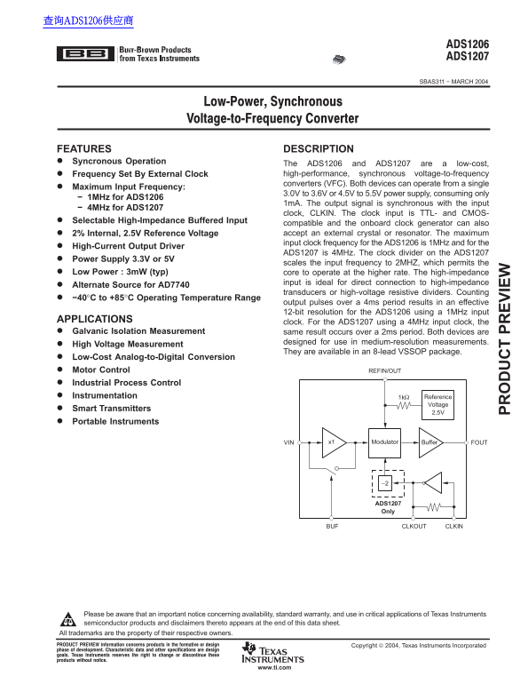
Page 1 Text Content
查询ADS1206供应商
SBAS311 − MARCH 2004
FEATURES DESCRIPTION Syncronous Operation
The ADS1206 and ADS1207 are a low-cost, Frequency Set By External Clock high-performance, synchronous voltage-to-frequency converters (VFC). Both devices can operate from a single
Maximum Input Frequency:
3.0V to 3.6V or 4.5V to 5.5V power supply, consuming only
− 1MHz for ADS1206
1m A. The output signal is synchronous with the input
− 4MHz for ADS1207
clock, CLKIN. The clock input is TTL- and CMOS-
Selectable High-Impedance Buffered Input
compatible and the onboard clock generator can also 2% Internal, 2.5V Reference Voltage accept an external crystal or resonator. The maximum input clock frequency for the ADS1206 is 1MHz and for the
High-Current Output Driver
ADS1207 is 4MHz. The clock divider on the ADS1207
Power Supply 3.3V or 5V
scales the input frequency to 2MHZ, which permits the
Low Power : 3m W (typ) core to operate at the higher rate. The high-impedance
input is ideal for direct connection to high-impedance
Alternate Source for AD7740
transducers or high-voltage resistive dividers. Counting
−40°C to +85°C Operating Temperature Range
output pulses over a 4ms period results in an effective 12-bit resolution for the ADS1206 using a 1MHz input
APPLICATIONS
clock. For the ADS1207 using a 4MHz input clock, the
Galvanic Isolation Measurement same result occurs over a 2ms period. Both devices are
designed for use in medium-resolution measurements.
High Voltage Measurement
They are available in an 8-lead VSSOP package.
Low-Cost Analog-to-Digital Conversion Motor Control REFIN/OUT Industrial Process Control Instrumentation 1kΩ Reference
Voltage
Smart Transmitters
Portable Instruments
Modulator Bufferx1 FOUTVIN
ADS1207 IE Only
BUF CLKOUT CLKIN
www.ti.com
Page Summary Contents For Texas Instruments ADS1206 ADS1207 Data Sheet Manual
Manual Details
| Brand | Texas Instruments |
|---|---|
| Pages | 8 |
| File Size | 153.75 KB |
| Published | June 21, 2026 |
Enter the captcha to get the download link:

Frequently Asked Questions
What is the operating temperature range for the ADS1206 and ADS1207?
Both devices operate within a temperature range of -40°C to +85°C.
How do I calculate resolution using the input clock frequency?
For ADS1206, 1MHz results in an effective 12-bit resolution over a 4ms period. For ADS1207, 4MHz results in the same result over a 2ms period.
What are the recommended supply voltage levels for these devices?
Low-voltage operation requires 3.0V to 3.6V, while high-voltage operation uses 4.5V to 5.5V.
Are there different packages available for purchasing?
The ADS1206 and ADS1207 are available in an 8-lead VSSOP package.