SANYO SCH1306 Handbook
Summary
This P-Channel Silicon MOSFET, SCH1306, is an ultrahigh-speed general-purpose switching device featuring low ON-resistance and 2.5V drive capability. Designed for reliable performance in demanding power applications, its comprehensive manual provides detailed electrical characteristics, including absolute maximum ratings, on-state resistance ($R_{on}$), capacitance values, and precise switching timings. This specialized component reference is essential for engineers and designers integrating high-performance switching circuitry into complex electronic systems.
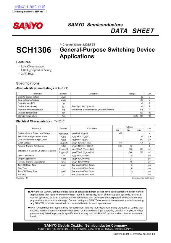
Page 1 Text Content
查询SCH1306供应商 Ordering number : ENN8101 SCH1306
P-Channel Silicon MOSFET
SCH1306 General-Purpose Switching Device Applications
Features Low ON-resistance. Ultrahigh-speed switching. 2.5V drive.
Specifications Absolute Maximum Ratings at Ta=25°C
Parameter Symbol Conditions Ratings Unit
Drain-to-Source Voltage VDSS --20 Gate-to-Source Voltage VGSS ±10 Drain Current (DC) ID --1 Drain Current (Pulse) IDP PW≤10µs, duty cycle≤1% --4 Allowable Power Dissipation PD Mounted on a ceramic board (900mm2✕0.8mm) 0.8 Channel Temperature Tch °C Storage Temperature Tstg --55 to +150 °C
Electrical Characteristics at Ta=25°C
Ratings
Parameter Symbol Conditions Unit
min typ max
Drain-to-Source Breakdown Voltage V(BR)DSS ID=--1m A, VGS=0 --20 Zero-Gate Voltage Drain Current IDSS VDS=--20V, VGS=0 --1 µA Gate-to-Source Leakage Current IGSS VGS=±8V, VDS=0 ±10 µA Cutoff Voltage VGS(off) VDS=--10V, ID=--1m A --0.4 --1.4 Forward Transfer Admittance yfs VDS=--10V, ID=--500m A 0.84 1.2
RDS(on)1 ID=--500m A, VGS=--4.0V mΩ
Static Drain-to-Source On-State Resistance
RDS(on)2 ID=--300m A, VGS=--2.5V mΩ
Input Capacitance Ciss VDS=--10V, f=1MHz p F Output Capacitance Coss VDS=--10V, f=1MHz p F Reverse Transfer Capacitance Crss VDS=--10V, f=1MHz p F Turn-ON Delay Time td(on) See specified Test Circuit. ns Rise Time tr See specified Test Circuit. ns Turn-OFF Delay Time td(off) See specified Test Circuit. ns Fall Time tf See specified Test Circuit. ns Marking : JF Continued on next page.
Any and all SANYO products described or contained herein do not have specifications that can handle applications that require extremely high levels of reliability, such as life-support systems, aircraft's control systems, or other applications whose failure can be reasonably expected to result in serious physical and/or material damage. Consult with your SANYO representative nearest you before using any SANYO products described or contained herein in such applications. SANYO assumes no responsibility for equipment failures that result from using products at values that exceed, even momentarily, rated values (such as maximum ratings, operating condition ranges, or other parameters) listed in products specifications of any and all SANYO products described or contained herein.
SANYO Electric Co.,Ltd. Semiconductor Company TOKYO OFFICE Tokyo Bldg., 1-10, 1 Chome, Ueno, Taito-ku, TOKYO, 110-8534 JAPAN
N1504PE TS IM TB-00000522 No.8101-1/4
Page Summary Contents For SANYO SCH1306 Handbook
Manual Details
| Brand | Sanyo |
|---|---|
| Pages | 4 |
| File Size | 36.68 KB |
| Published | May 28, 2026 |
Enter the captcha to get the download link:
