Philips Semiconductors SOT826-1 PCB Footprint Specifications User Guide
Summary
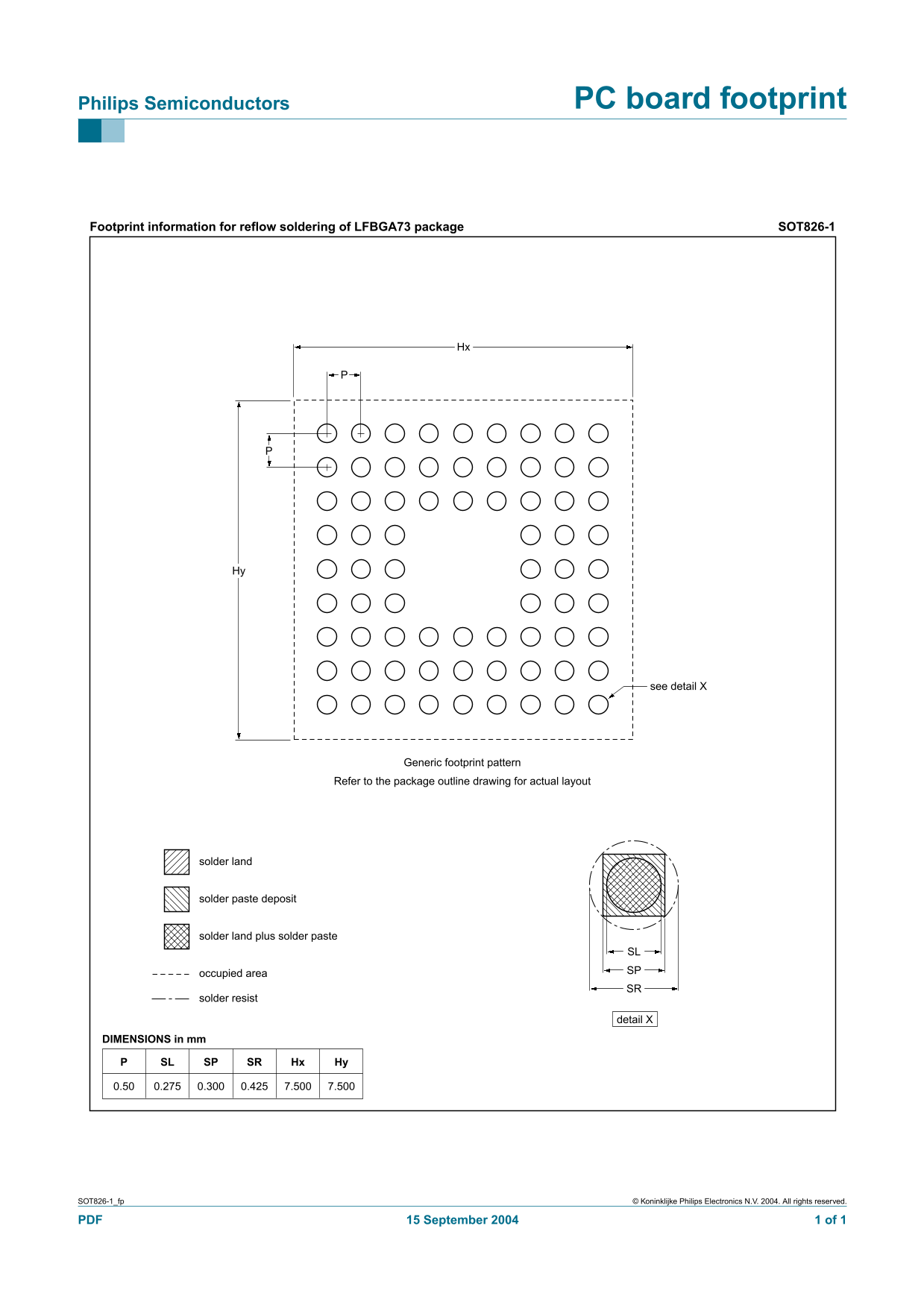
Essential resource providing the precise footprint pattern and detailed dimensional specifications (in mm) for SOT826-1 semiconductor components. This manual is vital reference material for PCB designers, electronics engineers, and manufacturing teams who require accurate guidelines for solder land preparation. It covers critical details for reflow soldering, including occupied areas and dedicated package outlines to ensure reliable component mounting and optimal electrical connection on your printed circuit board (PCB).
Page 1 Text Content
Philips Semiconductors PC board footprint
Footprint information for reflow soldering of LFBGA73 package SOT826-1
see detail X
Generic footprint pattern
Refer to the package outline drawing for actual layout
solder land
solder paste deposit
solder land plus solder paste
SL occupied area SP SR
solder resist
detail X
DIMENSIONS in mm
SL SP SR Hx Hy
SOT826-1_fp © Koninklijke Philips Electronics N.V. 2004. All rights reserved.
PDF 15 September 2004 1 of 1
Page Summary Contents For Philips Semiconductors SOT826-1 PCB Footprint Specifications User Guide
Manual Details
| Brand | Philips |
|---|---|
| Pages | 1 |
| File Size | 10.75 KB |
| Published | July 16, 2026 |
Enter the captcha to get the download link:

Frequently Asked Questions
What process is this footprint designed for?
This information is for reflow soldering of LFBGA73 package SOT826-1.
Where can I find the detailed physical layout pattern?
Users must refer to the package outline drawing for the actual layout details.
What are the critical dimensions listed in millimeters?
The key dimensions include PSL (0.50), SP (0.275), and SR (0.300) in mm.