Philips Semiconductors SOT751-2 PCB Board Footprint User Guide
Summary
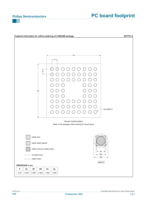
PCB footprint information for reflow soldering of the Philips LFBGA80 SOT751-2 package. Generic footprint pattern dimensions: 0.50mm pitch, solder land 0.275mm, solder paste deposit 0.300mm, solder resist opening 0.425mm, with 7.500mm x 7.500mm overall occupied area (Hx x Hy). Includes diagrams for solder land, solder paste, and occupied area with detail views. Reference to package outline drawing for actual layout. Copyright Koninklijke Philips Electronics 2004.
Page 1 Text Content
Philips Semiconductors PC board footprint
Footprint information for reflow soldering of LFBGA80 package SOT751-2
see detail X
Generic footprint pattern
Refer to the package outline drawing for actual layout
solder land
solder paste deposit
solder land plus solder paste
SL occupied area SP SR
solder resist
detail X
DIMENSIONS in mm
SL SP SR Hx Hy
SOT751-2_fp © Koninklijke Philips Electronics N.V. 2004. All rights reserved.
PDF 15 September 2004 1 of 1
Page Summary Contents For Philips Semiconductors SOT751-2 PCB Board Footprint User Guide
Manual Details
| Brand | Philips |
|---|---|
| Pages | 1 |
| File Size | 10.75 KB |
| Published | June 16, 2026 |
Enter the captcha to get the download link:
