Philips SC-75; SC-89 Footprint (REFLOW SOLDERING) Semiconductors PCB Board Footprint
Summary
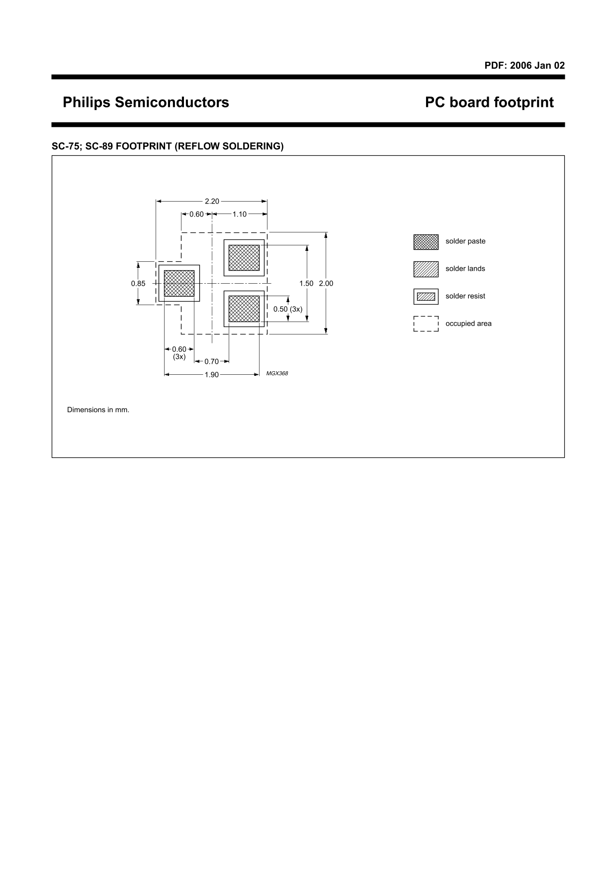
This essential technical guide provides precise specifications for semiconductor component footprints, including detailed dimensions for models like SC-75 and SC-89. It offers comprehensive instructions on optimal PCB design parameters, covering solder paste required areas, solder lands, and occupied space necessary for successful reflow soldering processes. Ideal for electronics engineers, PCB designers, and manufacturing professionals who require reliable standards for secure component mounting and accurate circuit board fabrication.
Page 1 Text Content
PDF: Jan
Philips Semiconductors PC board footprint
SC-75; SC-89 FOOTPRINT (REFLOW SOLDERING)
handbook, full pagewidth 2.20
solder paste
solder lands
solder resist
occupied area
1.90 MGX368
Dimensions in mm.
Page Summary Contents For Philips SC-75; SC-89 Footprint (REFLOW SOLDERING) Semiconductors PCB Board Footprint
Manual Details
| Brand | Philips |
|---|---|
| Pages | 1 |
| File Size | 7.72 KB |
| Published | July 07, 2026 |
Enter the captcha to get the download link:

Frequently Asked Questions
What specific component footprints does this guide cover?
The guide covers footprints SC-75 and SC-89.
Which soldering process is recommended for these footprints?
Reflow Soldering is specified for the footprint type.
What are the dimensions provided for solder lands?
Solder lands measurements include 0.85, 1.50, and 2.00 mm.
What is the recommended width for the solder resist?
The general size recommendation for solder resist is 0.50 (3x).