Philips Semiconductors SOT589-1 PC Board Footprint
Summary
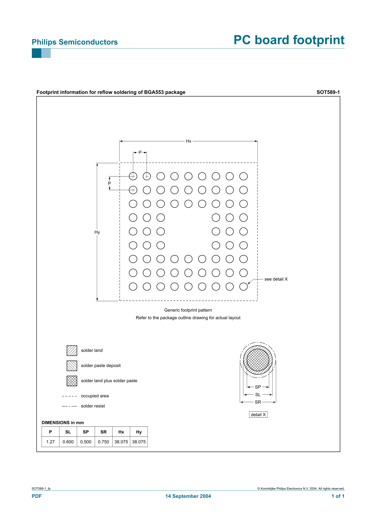
This is a comprehensive reference document detailing the precise PCB footprint specifications for assembling components packaged in the SOT589-1 format. It provides engineers with essential dimensional data, occupied area guidelines, and solder land patterns necessary for accurate reflow soldering. Use this manual to ensure optimal design and layout integrity when integrating BGA553 type semiconductors onto your Printed Circuit Board.
Page 1 Text Content
Philips Semiconductors PC board footprint
Footprint information for reflow soldering of BGA553 package SOT589-1
see detail X
Generic footprint pattern
Refer to the package outline drawing for actual layout
solder land
solder paste deposit
solder land plus solder paste
SP occupied area SL SR
solder resist
detail X
DIMENSIONS in mm
SL SP SR Hx Hy
SOT589-1_fp © Koninklijke Philips Electronics N.V. 2004. All rights reserved.
PDF 14 September 2004 1 of 1
Page Summary Contents For Philips Semiconductors SOT589-1 PC Board Footprint
Manual Details
| Brand | Philips |
|---|---|
| Pages | 1 |
| File Size | 10.94 KB |
| Published | July 07, 2026 |
Enter the captcha to get the download link:

Frequently Asked Questions
What is the package design for this component?
The part uses a SOT589-1 footprint, designed for reflow soldering of BGA553 packages.
How should I apply solder paste?
It requires the application of solder paste in defined areas as shown on the accompanying package outline drawing.
What are the key dimensions (in mm)?
The overall dimensions include PSL, SP, and SR measurements, with specific listings like 1.27, 0.600, and 0.500 mm for certain points.
Does this design support lead-free soldering?
The document is a footprint pattern for reflow soldering of BGA packages, indicating compatibility with standard electronic assembly processes.