Philips Semiconductors SOT307-2 PC Board Footprint Guide
Summary
Essential technical reference providing detailed footprint specifications for reflow soldering QFP44 packages. This comprehensive manual covers precise solder land dimensions, layout guides, and electrical parameters necessary for accurate PCB board integration. It is crucial for electronics engineers, hardware designers, and manufacturing teams who require optimal mounting solutions for semiconductor components using automated surface mount technology processes.
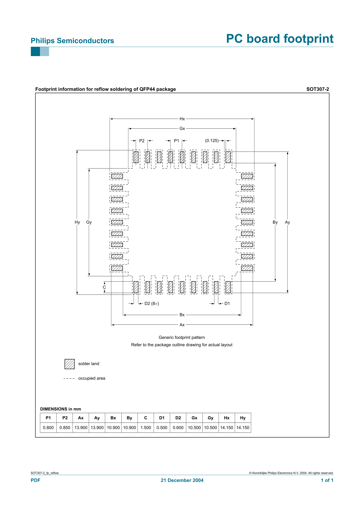
Page 1 Text Content
Philips Semiconductors PC board footprint
Footprint information for reflow soldering of QFP44 package SOT307-2
Gy Hy Ay By
Generic footprint pattern
Refer to the package outline drawing for actual layout
solder land
occupied area
DIMENSIONS in mm
P1 P2 Ax Ay Bx By D1 D2 Gx Gy Hx Hy
SOT307-2_fp_reflow © Koninklijke Philips Electronics N.V. 2004. All rights reserved.
PDF 21 December 2004 1 of 1
Page Summary Contents For Philips Semiconductors SOT307-2 PC Board Footprint Guide
Manual Details
| Brand | Philips |
|---|---|
| Pages | 1 |
| File Size | 10.90 KB |
| Published | July 12, 2026 |
Enter the captcha to get the download link:

Frequently Asked Questions
What is the primary function of this document?
It provides footprint information for reflow soldering of a QFP44 package SOT307-2.
What dimensions are provided for the footprint layout in millimeters?
The manual lists several dimensions, including 13.900/14.150 mm and 10.900/10.500 mm.
Do I need to use a generic pattern for mounting?
No, users should refer to the package outline drawing for the actual layout solder land occupied area dimensions.