Philips Semiconductors SOT623-1 PC board footprint User Guide
Summary
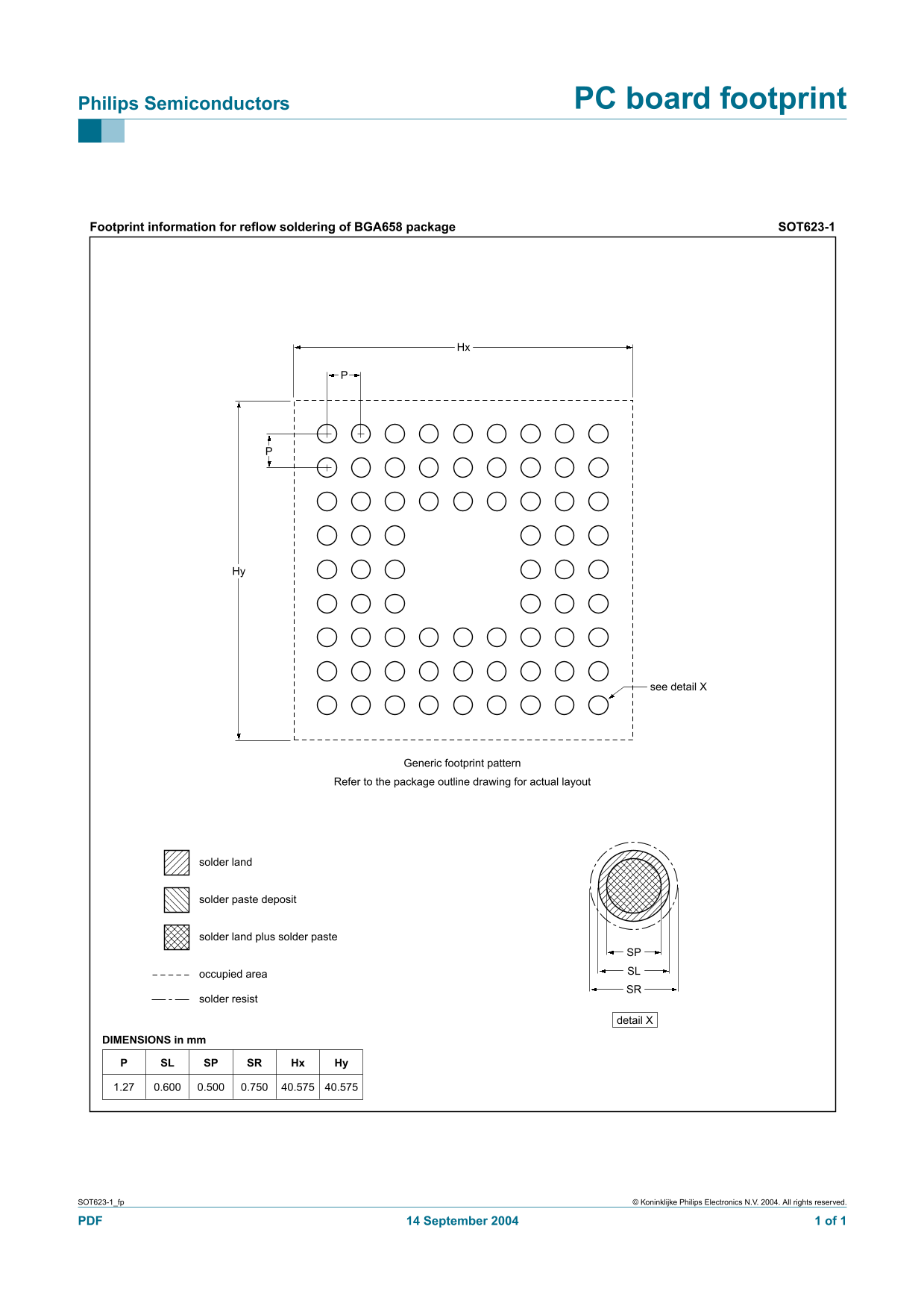
Essential technical documentation providing detailed footprint information for reliable circuit board design and manufacturing. This manual guides PCB engineers on generating accurate layouts for reflow soldering of BGA658 packages, specifically SOT623-1. It covers critical dimensions for solder land, paste deposit areas, and occupied zones, ensuring optimal component placement and high-quality electrical connections for PCB fabrication processes.
Page 1 Text Content
Philips Semiconductors PC board footprint
Footprint information for reflow soldering of BGA658 package SOT623-1
see detail X
Generic footprint pattern
Refer to the package outline drawing for actual layout
solder land
solder paste deposit
solder land plus solder paste
SP occupied area SL SR
solder resist
detail X
DIMENSIONS in mm
SL SP SR Hx Hy
SOT623-1_fp © Koninklijke Philips Electronics N.V. 2004. All rights reserved.
PDF 14 September 2004 1 of 1
Page Summary Contents For Philips Semiconductors SOT623-1 PC board footprint User Guide
Manual Details
| Brand | Philips |
|---|---|
| Pages | 1 |
| File Size | 10.94 KB |
| Published | July 07, 2026 |
Enter the captcha to get the download link:

Frequently Asked Questions
What is the footprint used for reflow soldering?
The footprint provided is intended for reflow soldering of a BGA658 package in SOT623-1 style.
Can I use this board pattern for general circuitry?
No, the drawing shows a specific footprint pattern (SOT623-1_fp) and should be referenced with detailed package drawing rather than used generally.
Are there specific dimensions to be aware of?
Yes, key dimensions include 40.575 mm for the total length/width; occupied areas are described by PSL, SP, and SR notations.
What year was this technical document created?
The document date shown is September 14, 2004, and it references Philips Electronics N.V. copyright.