Philips Semiconductors SOT532-1 PCB Footprint Specification User Guide
Summary
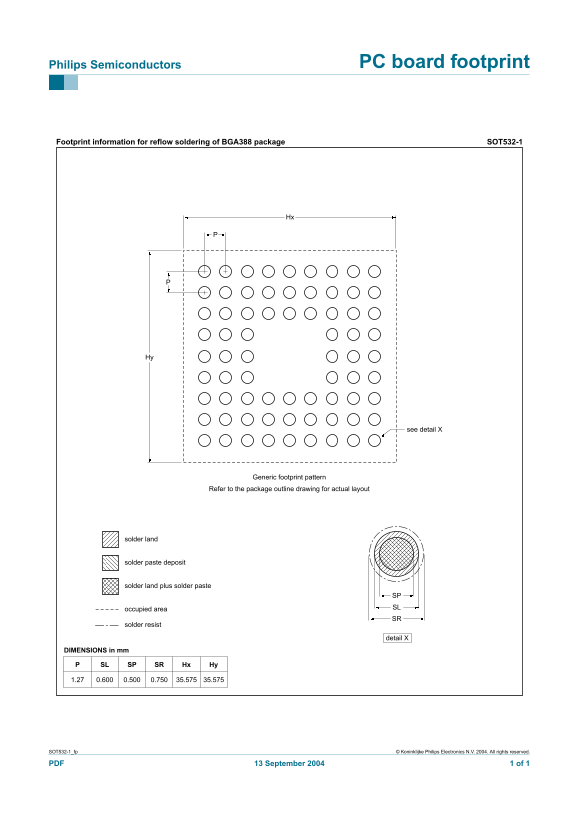
PCB footprint information for reflow soldering of the Philips BGA388 SOT532-1 package. Generic footprint pattern with 1.27mm pitch, solder land 0.600mm, solder paste deposit 0.500mm, solder resist opening 0.750mm, and overall occupied area 35.575mm x 35.575mm. Includes detail views for solder land plus paste occupied area and solder resist dimensions. Reference to package outline drawing for actual layout specifications. Copyright Koninklijke Philips Electronics 2004.
Page 1 Text Content
Philips Semiconductors PC board footprint
Footprint information for reflow soldering of BGA388 package SOT532-1
see detail X
Generic footprint pattern
Refer to the package outline drawing for actual layout
solder land
solder paste deposit
solder land plus solder paste
SP occupied area SL SR
solder resist
detail X
DIMENSIONS in mm
SL SP SR Hx Hy
SOT532-1_fp © Koninklijke Philips Electronics N.V. 2004. All rights reserved.
PDF 13 September 2004 1 of 1
Page Summary Contents For Philips Semiconductors SOT532-1 PCB Footprint Specification User Guide
Manual Details
| Brand | Philips |
|---|---|
| Pages | 1 |
| File Size | 10.94 KB |
| Published | June 17, 2026 |
Enter the captcha to get the download link:

Frequently Asked Questions
What package footprint information does this guide provide?
It provides the footprint information for reflow soldering of BGA388 packages referenced as SOT532-1.
Where should I refer to determine the final layout pattern?
You must refer to the package outline drawing for the actual layout and solder land details.
What units are used for the specified dimensions (PSL, SP, SR, Hx, Hy)?
All listed dimensional measurements are provided in millimeters (mm).