# A B C D E F G H I J K L M N O P Q R S T U V W X Y Z

PHILIPS BSH112 User Guide and Data Sheet

Summary

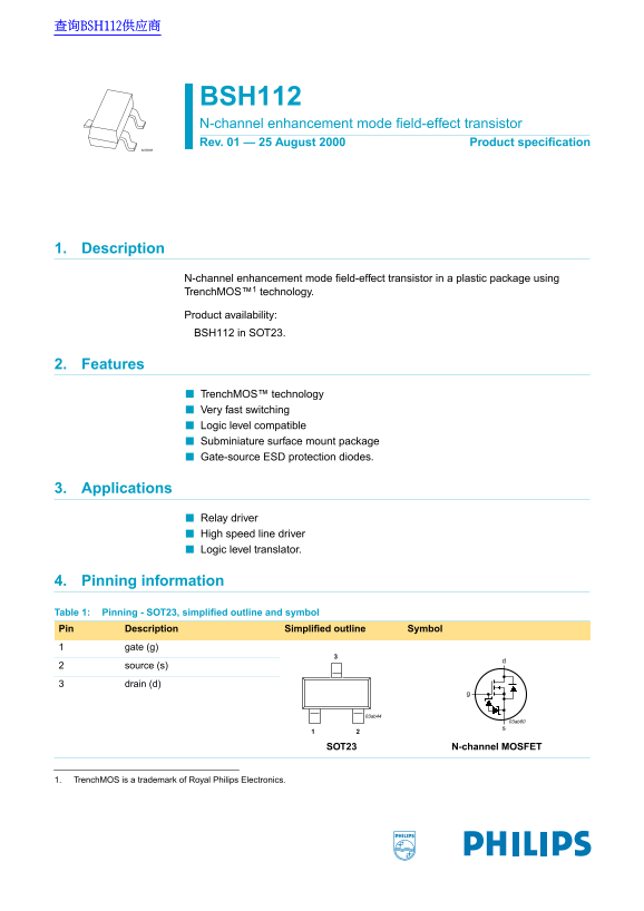
BSH112 is an N-channel enhancement mode MOSFET using TrenchMOS technology in a compact SOT23 package. Ideal for relay drivers, high-speed line drivers, and logic level translators, this surface mount device features fast switching, logic-level compatibility, and gate-source ESD protection diodes.
📄 Preview PAGE OF 13

Page 1 Text Content

查询BSH112供应商

BSH112 N-channel enhancement mode field-effect transistor Rev. 01 — 25 August 2000 Product specification M3D088

1. Description

N-channel enhancement mode field-effect transistor in a plastic package using Trench MOS™1 technology.

Product availability: BSH112 in SOT23.

2. Features

Trench MOS™ technology Very fast switching Logic level compatible Subminiature surface mount package Gate-source ESD protection diodes.

3. Applications

Relay driver High speed line driver Logic level translator.

4. Pinning information Table 1: Pinning - SOT23, simplified outline and symbol Pin Description Simplified outline Symbol

gate (g) source (s) drain (d)

03ab44

03ab60

SOT23 N-channel MOSFET

1. Trench MOS is a trademark of Royal Philips Electronics.

Page Summary Contents For PHILIPS BSH112 User Guide and Data Sheet

Page 1 查询BSH112供应商 BSH112 N-channel enhancement mode field-effect transistor Rev. 01 — 25 August 2000 Product specification M3D088 1. Description N-channel enhancement mode field-effect transistor in a plast...
Page 2 Philips Semiconductors BSH112 N-channel enhancement mode field-effect transistor 5. Quick reference data Table 2: Quick reference data Symbol Parameter Conditions Typ Max Unit VDS drain-source voltage...
Page 3 Philips Semiconductors BSH112 N-channel enhancement mode field-effect transistor 03aa17 03aa25 Tsp (o C) Tsp (o C) Ptot VGS 4.5 Pder 100%×= tot C°( Ider 100%×= Fig 1. Normalized total power dissipatio...
Page 4 Philips Semiconductors BSH112 N-channel enhancement mode field-effect transistor 7. Thermal characteristics Table 4: Thermal characteristics Symbol Parameter Conditions Value Unit Rth(j-sp) thermal re...
Page 5 Philips Semiconductors BSH112 N-channel enhancement mode field-effect transistor 8. Characteristics Table 5: Characteristics Tj °C unless otherwise specified Symbol Parameter Conditions Min Typ Max Un...
Page 6 Philips Semiconductors BSH112 N-channel enhancement mode field-effect transistor 03aa41 03aa43 ID Tj = 25o C VGS = 10V VDS > ID X RDSon 4.5 V Tj = 25o C VDS (V) VGS (V) Tj °C Tj °C and 150 °C; VDS ...
Page 7 Philips Semiconductors BSH112 N-channel enhancement mode field-effect transistor 03aa34 03aa37 10-1 VGS(th) ID (A) typmin min 10-4 o C) Tj ( VGS (V) ID m A; VDS VGS Tj °C; VDS Fig 9. Gate-source thres...
Page 8 Philips Semiconductors BSH112 N-channel enhancement mode field-effect transistor 03aa45 VGS = 0 V Tj = 25o C VSD (V) Tj °C and 150 °C; VGS Fig 13. Source (diode forward) current as a function of sourc...
Page 9 Philips Semiconductors BSH112 N-channel enhancement mode field-effect transistor 9. Package outline Plastic surface mounted package; 3 leads SOT23 e1 bp Lp detail X scale DIMENSIONS (mm are the origin...
Page 10 Philips Semiconductors BSH112 N-channel enhancement mode field-effect transistor 10. Revision history Table 6: Revision history Rev Date CPCN Description Product specification; initial version. 9397 7...
Page 11 Philips Semiconductors BSH112 N-channel enhancement mode field-effect transistor 11. Data sheet status Datasheet status Product status Definition Objective specification Development This data sheet co...
Page 12 Philips Semiconductors BSH112 N-channel enhancement mode field-effect transistor Philips Semiconductors - a worldwide company Argentina: see South America Netherlands: Tel. +31 2785, Fax. +31 Australi...
Page 13 Philips Semiconductors BSH112 N-channel enhancement mode field-effect transistor Contents Description . . . . . . . . . . . . . . . . . . . . . . . . . . . . . Features . . . . . . . . . . . . . . . ....

Manual Details

Brand Philips
Pages 13
File Size 112.68 KB
Published June 20, 2026
7 views

Enter the captcha to get the download link:

captcha

Frequently Asked Questions

What is the maximum drain-source voltage and continuous drain current for BSH112?

Maximum VDS is 60 V (DC) and continuous ID is 300 mA at 25 °C with VGS = 10 V.

What is the typical on-state resistance of BSH112?

At VGS = 10 V and ID = 500 mA, typical RDSon is 2.8 Ω (max 5 Ω); at VGS = 4.5 V and ID = 75 mA, typical is 3.8 Ω (max 5.3 Ω).

In which package is BSH112 available?

BSH112 is available in a SOT23 surface mount package with gate, source, and drain pins.

What are typical applications of BSH112?

Typical applications include relay driver, high speed line driver, and logic level translator.

What is the operating junction temperature range for BSH112?

The operating junction temperature range is -65 °C to +150 °C.