# A B C D E F G H I J K L M N O P Q R S T U V W X Y Z

Panasonic AN8049SH Data Manual

Summary

The AN8049SH is a high-efficiency, 3-channel PWM DC-DC converter control IC designed for complex power supply systems. It provides versatile regulation with two step-up and one polarity inverting output, featuring ultra-low voltage capability down to 1.8V (suitable for dry batteries) and support up to 14V operation. The comprehensive manual serves as an essential resource for engineers, detailing the IC’s pin configurations, operational limits, control sequence methods, and providing detailed application circuit examples necessary for designing reliable and miniaturized electronic power solutions.
📄 Preview PAGE OF 28

Page 1 Text Content

查询AN8049供应商 Voltage Regulators

AN8049SH 1.8-volt 3-channel step-up, step-down, and polarity inverting DC-DC converter control IC

Unit : mm

Overview

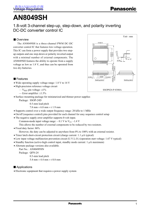
The AN8049SH is a three-channel PWM DC-DC converter control IC that features low-voltage operation. This IC can form a power supply that provides two step- up outputs and one step-down or polarity inverted output with a minimal number of external components. The

0° to 10°

AN8049SH features the ability to operate from a supply voltage as low as 1.8 V, and thus can be operated from two dry-batteries.

Features

Seating plane Seating plane

Wide operating supply voltage range: 1.8 V to 14 V High-precision reference voltage circuit

VREF pin voltage: ±1% SSOP024-P-0300A

Error amplifier: ±1.5% Surface mounting package for miniaturized and thinner power supplies Package: SSOP-24D 0.5-mm lead pitch 7.8 mm × 6.8 mm × t 1.9 mm

Supports control over a wide output frequency range: 20 k Hz to 1 MHz 5. 5± 0. 0. ±0 .1 0. ±0 .1 7. 5± 0.

On/off (sequence control) pins provided for each channel for easy sequence control setup 0. 1± 0. 1. 5± 0.

The negative supply error amplifier supports 0-volt input. Common-mode input voltage range: − 0.1 V to VCC −1.4 V This allows the number of external components to be reduced by two resistors. Fixed duty factor: 86% However, the duty can be adjusted to anywhere from 0% to 100% with an external resistor. Timer latch short-circuit protection circuit (charge current: 1.1 µA typical) Low input voltage malfunction prevention circuit (U.V.L.O.) (operation start voltage: 1.67 V typical) Standby function (active-high control input, standby mode current: 1 µA maximum) Alternate package versions also available. Part No.: AN8049FHN Package: QFN-24

0.5-mm lead pitch 5.4 mm × 4.4 mm × t 0.8 mm

Applications Electronic equipment that requires a power supply system

Page Summary Contents For Panasonic AN8049SH Data Manual

Page 1 查询AN8049供应商 Voltage Regulators AN8049SH 1.8-volt 3-channel step-up, step-down, and polarity inverting DC-DC converter control IC Unit : mm Overview The AN8049SH is a three-channel PWM DC-DC converter ...
Page 2 AN8049SH Voltage Regulators Block Diagram IN −2 IN -1 Reference voltage Sawtooth wave generator supply VREF VCCOn/off 0.3 V FB (Allowance: ±1%) control Error 20 kΩ amplifier 1 OUT1 1. µA S.C.P. comp. ...
Page 3 Voltage Regulators AN8049SH Absolute Maximum Ratings Parameter Symbol Rating Unit Supply voltage VCC 14.2 Off pin allowable application VOFF 14.2 voltage CTL pin allowable application VCTL VCC − 0.2 v...
Page 4 AN8049SH Voltage Regulators Electrical Characteristics at VCC = 2.4 V, CREF = 0.1 µF, Ta = 25°C Parameter Symbol Conditions Min Typ Max Unit Reference voltage block Reference voltage VREF IREF = − 0.1...
Page 5 Voltage Regulators AN8049SH Electrical Characteristics at VCC = 2.4 V, CREF = 0.1 µF, Ta = 25°C (continued) Parameter Symbol Conditions Min Typ Max Unit Output 1 block Output duty factor 1 Du1 RT = 7....
Page 6 AN8049SH Voltage Regulators Electrical Characteristics at Ta = 25°C (continued) Design reference data Note: The characteristics listed below are reference values related to the IC design and are not g...
Page 7 Voltage Regulators AN8049SH Terminal Equivalent Circuits Pin No. Equivalent circuit Description I/O Connection for the capacitor that sets the timer latch short-circuit protection 1.1 µA circuit time ...
Page 8 AN8049SH Voltage Regulators Terminal Equivalent Circuits (continued) Pin No. Equivalent circuit Description I/O CTL3: Controls the on/off state of channel 3. A delay can be provided in the power suppl...
Page 9 Voltage Regulators AN8049SH Terminal Equivalent Circuits (continued) Pin No. Equivalent circuit Description I/O Off: Controls the on/off state. Start and stop of When the input is high: normal interna...
Page 10 AN8049SH Voltage Regulators Terminal Equivalent Circuits (continued) Pin No. Equivalent circuit Description I/O See pin 10. OUT2: Push-pull output. The absolute maximum rating for the output source cu...
Page 11 Voltage Regulators AN8049SH Terminal Equivalent Circuits (continued) Pin No. Equivalent circuit Description I/O IN−2: Inverting input to the error amplifier 2. FB2: Output from the error amplifier 2. ...
Page 12 AN8049SH Voltage Regulators Usage Notes [1] Allowable power dissipation 1. Since the power dissipation (P) in this IC increases proportionally with the supply voltage, applications must be careful to ...
Page 13 Voltage Regulators AN8049SH Usage Notes (continued) [3] Notes on MOS drive Since the AN8049SH channel 1 and 2 output circuits were designed to drive bipolar transistors, the following points require c...
Page 14 AN8049SH Voltage Regulators Application Notes (continued) [2] Main characteristics Timing capacitance  Oscillator frequency DT1 and DT2 pin voltage  Maximum on-duty 1M f = 190 k Hz RT = 3 kΩ f = 1 M...
Page 15 Voltage Regulators AN8049SH Application Notes (continued) (m SO (O [2] Main characteristics (continued) RB  ISO(OUT) RB  ISI(OUT) −20 VCC = 1.8 V −30 VCC = 14 V RB (Ω) RB (Ω) I( (m
Page 16 AN8049SH Voltage Regulators Application Notes (continued) [3] Timing charts VCC pin voltage waveform 1.67 V Output short S.C.P. pin voltage waveform CTL pin voltage waveform FB OSC DT OUT1/2 pin volta...
Page 17 Voltage Regulators AN8049SH Application Notes (continued) [4] Function descriptions 1. Reference voltage block This circuit is composed of a band gap circuit, and outputs a 1.26 V (typical) reference ...
Page 18 AN8049SH Voltage Regulators Application Notes (continued) [4] Function descriptions (continued) 4. Error amplifier 2 FB2 This circuit is an npn-transistor input error amplifier that detects and amplif...
Page 19 Voltage Regulators AN8049SH Application Notes (continued) [4] Function descriptions (continued) 7. Low input voltage malfunction prevention circuit (U.V.L.O.) This circuit protects the system against ...
Page 20 AN8049SH Voltage Regulators Application Notes (continued) [5] Time constant setup for the timer latch short-circuit protection circuit Figure 6 shows the structure of the timer latch short-circuit pro...
Page 21 Voltage Regulators AN8049SH Application Notes (continued) [6] Setting the maximum duty The maximum duty is set to 86% internally to the IC. However, this setting can be changed to be any value in the ...
Page 22 AN8049SH Voltage Regulators Application Notes (continued) [7] Setting the soft start time The soft start time is determined by the value of the capacitor connected between the DT pin and ground. OSC p...
Page 23 Voltage Regulators AN8049SH Application Notes (continued) [8] Parallel synchronous operation of multiple ICs Multiple instances of this IC can be operated in parallel. If the OSC pins (pin 17) and OFF...
Page 24 AN8049SH Voltage Regulators Application Notes (continued) [9] Sequential operation Sequential operation under the control of external capacitors Delays can be provided in the startup times by insertin...
Page 25 Voltage Regulators AN8049SH Application Notes (continued) [10] Notes on power supply printed circuit board design Careful attention must be paid to the following points when designing the printed circ...
Page 26 AN8049SH Voltage Regulators Application Notes (continued) [11] Differences between this IC and the AN8049FHN The pin arrangements differ. The AN8049FHN is a alternative package version of this IC. S. ...
Page 27 Voltage Regulators AN8049SH Application Notes (continued) [12] Error amplifier frequency characteristics 1. Error amplifiers 1 and 2 (Test circuit) IN−1 VOUT 100 kΩ FB1 VREF −20 Ph as °) ai d B )Amp.1...
Page 28 AN8049SH Voltage Regulators Application Circuit Example In ve rt in 0. µF St ep -u Input 10 kΩ 10 kΩ OUT2 OUT1 GND RB1 OUT3 RB2 St ep -d ow 1 kΩ VCC VREF 0.12 µF OSC Off 7.5 kΩ n/ ff IN+3 CTL1 IN−3 CT...

Manual Details

Brand Panasonic
Pages 28
File Size 256.82 KB
Published June 21, 2026
10 views

Enter the captcha to get the download link:

captcha

Frequently Asked Questions

What is the minimum input voltage for the AN8049SH?

The IC supports a wide operating supply voltage range, from 1.8 V to 14 V.

How many outputs does this converter control IC provide?

It is a three-channel PWM DC-DC converter control IC that provides two step-up and one step-down or polarity inverted output.

What is the operating temperature range for the AN8049SH?

The device operates from -30°C to +85°C. (Storage temperature: -55°C to +125°C).