National Semiconductor MN54F189-X REV 1A0 Data Sheet Manual
Summary
Discover this high-speed, robust 64-bit Random Access Memory (RAM) chip, engineered for critical data storage in demanding applications. Featuring reliable 3-state outputs and buffered inputs, the F189 provides stable performance across extreme temperature ranges. This technical manual covers comprehensive electrical characteristics, detailed timing parameters (AC/DC), and rigorous military-grade qualification standards (MIL-STD). It is essential documentation for hardware designers, electronics engineers, and system integrators requiring high-reliability memory components for embedded or industrial systems.
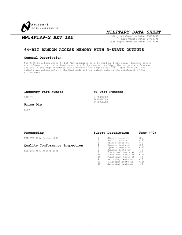
Page 1 Text Content
MILITARY DATA SHEET Original Creation Date: 05/17/96
MN54F189-X REV 1A0
Last Update Date: 07/30/96
Last Major Revision Date: 05/17/96
64-BIT RANDOM ACCESS MEMORY WITH 3-STATE OUTPUTS General Description The F189 is a high-speed 64-bit RAM organized as a 16-word by 4-bit array. Address inputs are buffered to minimize loading and are fully decoded on-chip. The outputs are 3-state and are in the high impedance state whenever the Chip Select (CS) input is HIGH. The outputs are active only in the Read mode and the output data is the complement of the stored data.
Industry Part Number NS Part Numbers 54F189 54F189DLQB
54F189FLQB 54F189LLQB
Prime Die M189
Processing Subgrp Description Temp ( C)o MIL-STD-883, Method 5004 Static tests at +25
Static tests at +125 Static tests at -40 Quality Conformance Inspection Dynamic tests at +25 Dynamic tests at +125 Dynamic tests at -40
MIL-STD-883, Method 5005
Functional tests at +25
8A Functional tests at +125 8B Functional tests at -40
Switching tests at +25 Switching tests at +125 Switching tests at -40
Page Summary Contents For National Semiconductor MN54F189-X REV 1A0 Data Sheet Manual
Manual Details
| Brand | National |
|---|---|
| Pages | 6 |
| File Size | 18.45 KB |
| Published | June 04, 2026 |
Enter the captcha to get the download link:

Frequently Asked Questions
What is the recommended operating temperature range for military use?
The recommended operating condition for military environments is -40 C to +125 C.
How are data inputs protected in this RAM module?
It features buffered and diode-clamped inputs to minimize loading and ringinhg.
Does the output state indicate the stored data directly?
No, on the outputs, the data provided is the complement of the stored data.
What are the typical access times for different operations?
The minimum access time (tpLH) at 25C ranges from 9.0 to 13.5 ns depending on the operation (An or CS).