National Semiconductor MN54ABT244-X REV 0B0 Data Sheet
Summary
Engineers can utilize this octal buffer and line driver for robust high-speed bus applications, functioning efficiently as a critical address or clock transmitter/receiver. This comprehensive manual details operational parameters, including stringent performance data for output sink capability and guaranteeing reliable function across extreme temperature ranges (-55°C to +125°C). It provides essential electrical characteristics, absolute maximum ratings, and detailed switching specifications needed for precise circuit design.
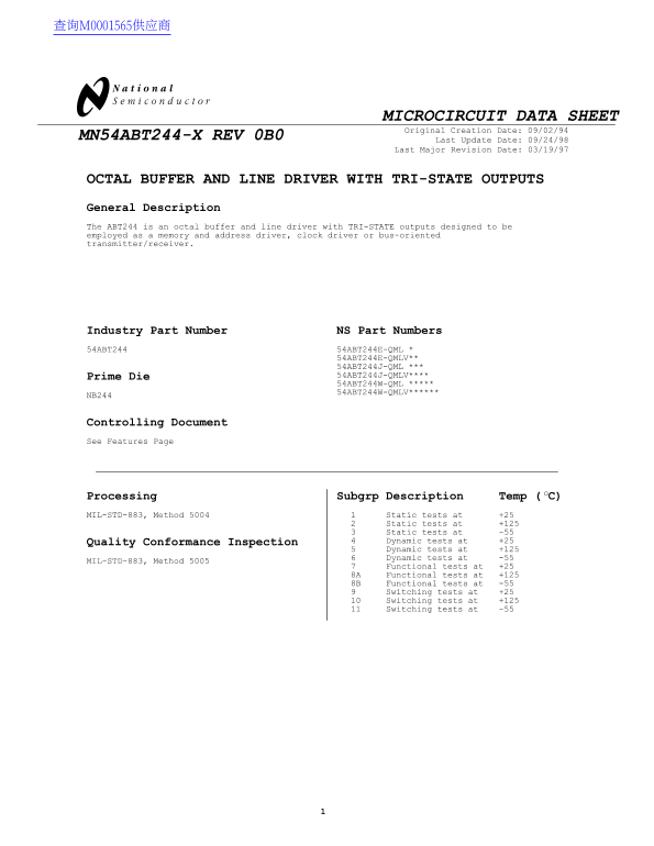
Page 1 Text Content
MICROCIRCUIT DATA SHEET Original Creation Date: 09/02/94
MN54ABT244-X REV 0B0
Last Update Date: 09/24/98
Last Major Revision Date: 03/19/97
OCTAL BUFFER AND LINE DRIVER WITH TRI-STATE OUTPUTS General Description The ABT244 is an octal buffer and line driver with TRI-STATE outputs designed to be employed as a memory and address driver, clock driver or bus-oriented transmitter/receiver.
Industry Part Number NS Part Numbers 54ABT244 54ABT244E-QML *
54ABT244E-QMLV** 54ABT244J-QML *** Prime Die 54ABT244J-QMLV**** 54ABT244W-QML ***** 54ABT244W-QMLV******
NB244
Controlling Document See Features Page
Processing Subgrp Description Temp ( C)o MIL-STD-883, Method 5004 Static tests at +25
Static tests at +125 Static tests at -55 Quality Conformance Inspection Dynamic tests at +25 Dynamic tests at +125 Dynamic tests at -55
MIL-STD-883, Method 5005
Functional tests at +25
8A Functional tests at +125 8B Functional tests at -55
Switching tests at +25 Switching tests at +125 Switching tests at -55
Page Summary Contents For National Semiconductor MN54ABT244-X REV 0B0 Data Sheet
Manual Details
| Brand | National |
|---|---|
| Pages | 13 |
| File Size | 210.10 KB |
| Published | June 18, 2026 |
Enter the captcha to get the download link:

Frequently Asked Questions
What are the primary applications for the ABT244 device?
The chip is designed to function as a memory and address driver, clock driver, or bus-oriented transmitter/receiver.
What is the recommended supply voltage range (Vcc)?
The optimal operating condition specifies a supply voltage (Vcc) between 4.5V and 5.5V.
How much output current can this device handle?
It features an output sink capability of 48mA and a source capability of 24mA.
Does the device include protective measures?
Yes, it guarantees latchup protection and provides high impedance glitch free bus loading during power cycles.