# A B C D E F G H I J K L M N O P Q R S T U V W X Y Z

NATIONAL SEMICONDUCTOR LMV225 LMV226 LMV228 Owner's Manual

Summary

These RF power detectors are essential integrated circuits designed for precise measurement of RF power in CDMA and WCDMA applications across the 450 MHz to 2 GHz spectrum. They feature a wide 30 dB linear detection range, multi-band capabilities, and temperature compensation, making them ideal for advanced wireless communication systems. The manual provides comprehensive electrical specifications, operational details, and application guidance for engineers specializing in cellular network infrastructure and RF power control design.
📄 Preview 📖 Table of Contents Contents PAGE OF 20

Page 1 Text Content

August

LM 225/LM 226/LM ow er etector for and in icro

LMV225/LMV226/LMV228 RF Power Detector for CDMA and WCDMA in micro SMD General Description Features

The LMV225/LMV226/LMV228 are 30d B RF power detec- d B linear in d B power detection range tors intended for use in CDMA and WCDMA applications. Output voltage range 0.2 to 2V

The device has an RF frequency range from MHz to Logic low shutdown GHz. It provides an accurate temperature and supply com-

Multi-band operation from MHz to MHz

pensated output voltage that relates linearly to the RF input

Accurate temperature compensation

power in d Bm. The circuit operates with single supply from

micro SMD package 1.0 mm 1.0 mm 0.6 mm

2.7V to 5.5V. The LMV225/LMV226/LMV228 have an inte- grated filter for low-ripple average power detection of CDMA

Applications

signals with d B dynamic range. Additional filtering can be

applied using single external capacitor. CDMA RF power control The LMV225 has an RF power detection range from –30 WCDMA RF power control d Bm to d Bm and is ideally suited for direct use in combi- CDMA2000 RF power control

nation with resistive taps. The LMV226/LMV228 have de- PA modules tection range from –15 d Bm to d Bm and are intended for use in combination with directional coupler. The LMV226 is equipped with buffered output which makes it suitable for GSM, EDGE, GPRS and TDMA applications. The device is active for Enable HI, otherwise it is in low power consumption shutdown mode. During shutdown the output will be LOW. The output voltage ranges from 0.2V to 2V and can be scaled down to meet ADC input range re- quirements. The LMV225/LMV226/LMV228 power detectors are offered in the small 1.0 mm 1.0 mm 0.6 mm micro SMD pack- age.

Typical Application

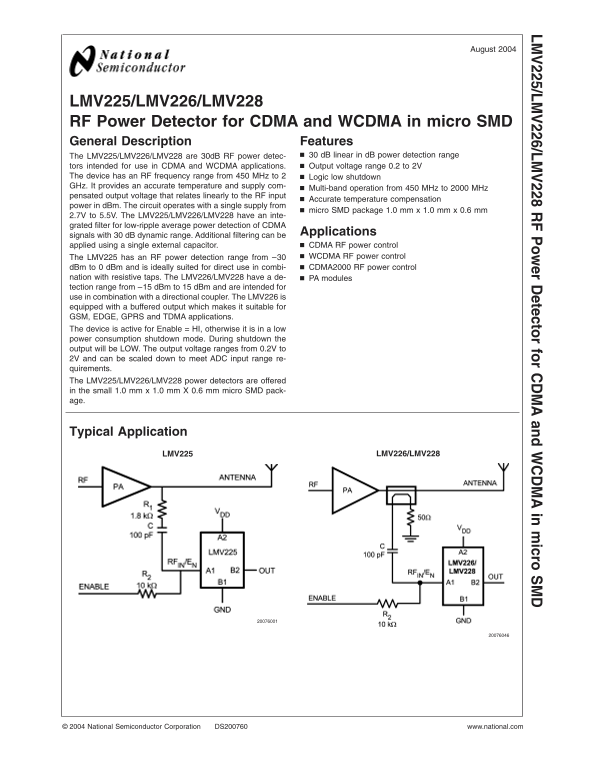
LMV225 LMV226/LMV228

National Semiconductor Corporation DS200760 www.national.com

Page Summary Contents For NATIONAL SEMICONDUCTOR LMV225 LMV226 LMV228 Owner's Manual

Page 1 August LM 225/LM 226/LM ow er etector for and in icro LMV225/LMV226/LMV228 RF Power Detector for CDMA and WCDMA in micro SMD General Description Features The LMV225/LMV226/LMV228 are 30d B RF power de...
Page 2 Absolute Maximum Ratings (Note 1) Junction Temperature (Note 3) 150˚C Max If Military/Aerospace specified devices are required, Mounting Temperature LM 5/ LM 6/ LM please contact the National Semicond...
Page 3 2.7 DC and AC Electrical Characteristics (Continued) LM Unless 225/LM otherwise 226/LM specified, all limits are guaranteed to VDD 2.7V; TJ 25˚C. Boldface limits apply at temperature extremes. (Note 4...
Page 4 2.7 DC and AC Electrical Characteristics (Continued) Unless otherwise specified, all limits are guaranteed to VDD 2.7V; TJ 25˚C. Boldface limits apply at temperature extremes. LM 5/ LM 6/ LM (Note 4) ...
Page 5 5.0 DC and AC Electrical Characteristics (Continued) LM Unless 225/LM otherwise 226/LM specified, all limits are guaranteed to VDD 5.0V; TJ 25˚C. Boldface limits apply at temperature extremes. (Note 4...
Page 6 5.0 DC and AC Electrical Characteristics (Continued) Unless otherwise specified, all limits are guaranteed to VDD 5.0V; TJ 25˚C. Boldface limits apply at temperature extremes. LM 5/ LM 6/ LM (Note 4) ...
Page 7 Connection Diagram LM 225/LM 226/LM 4-Bump micro SMD Pin Description Pin Name Description Power Supply A2 VDD Positive Supply Voltage B1 GND Power Ground A1 RFIN/EN DC voltage determines enable state ...
Page 8 Block Diagrams LM 5/ LM 6/ LM LMV225 LMV226 LMV228 www.national.com
Page 9 Typical Performance Characteristics Unless otherwise specified, VDD 2.7V, TJ 25˚C. LM 225/LM 226/LM Supply Current vs. Supply Voltage (LMV225) Supply Current vs. Supply Voltage (LMV226) Supply Current...
Page 10 Typical Performance Characteristics Unless otherwise specified, VDD 2.7V, TJ 25˚C. (Continued) LM 5/ LM 6/ LM Output Voltage and Log Conformance vs. Output Voltage and Log Conformance vs. RF Input Pow...
Page 11 Typical Performance Characteristics Unless otherwise specified, VDD 2.7V, TJ LM 25˚C. 225/LM (Continued) 226/LM Output Voltage and Log Conformance vs. Output Voltage and Log Conformance vs. RF Input P...
Page 12 Typical Performance Characteristics Unless otherwise specified, VDD 2.7V, TJ 25˚C. (Continued) LM 5/ LM 6/ LM Logarithmic Slope vs. Frequency (LMV225) Logarithmic Slope vs. Frequency (LMV226) Logarith...
Page 13 Typical Performance Characteristics Unless otherwise specified, VDD 2.7V, TJ LM 25˚C. 225/LM (Continued) 226/LM Output Variation vs. RF Input Power Normalized to 25˚C Output Variation vs. RF Input Pow...
Page 14 Typical Performance Characteristics Unless otherwise specified, VDD 2.7V, TJ 25˚C. (Continued) LM 5/ LM 6/ LM Output Variation vs. RF Input Power Normalized to 25˚C Output Variation vs. RF Input Power...
Page 15 Typical Performance Characteristics Unless otherwise specified, VDD 2.7V, TJ LM 25˚C. 225/LM (Continued) 226/LM RF Input Impedance vs. Frequency Resistance and PSRR vs. Frequency (LMV225, LMV226 and L...
Page 16 Solving this expression for R1, using that RIN 50Ω, yields: Application Notes LM 5/ LM 6/ LM CONFIGURING TYPICAL APPLICATION The LMV225/LMV226/LMV228 are power detectors in- tended for CDMA and WCDMA ...
Page 17 Application Notes (Continued) LM 225/LM 226/LM number. The goal is to have magnitude transfer, which is sufficiently flat in the used frequency range; capacitor should be chosen significantly larger t...
Page 18 Application Notes 1.5 n F capacitor is then log (200/12) 24.4 d B. This (Continued) is very close to the calculated number of the previous para- LM 5/ LM 6/ LM graph. FIGURE 6. Output Ripple vs. RF In...
Page 19 Application Notes Figure shows logarithmic function on logarithmic (Continued) scale and the piecewise approximation of the logarithmic LM 225/LM 226/LM function. FIGURE 8. Gain Cell All gain cell out...
Page 20 Physical Dimensions inches (millimeters) unless otherwise noted LM 5/ LM 6/ LM ow er et ec to fo an in ic ro NOTES: UNLESS OTHERWISE SPECIFIED 1. EPOXY COATING 2. Sn/37Pb EUTECTIC BUMP 3. RECOMMEND NO...

Manual Details

Brand National
Pages 20
File Size 649.05 KB
Published June 17, 2026
4 views

Enter the captcha to get the download link:

captcha

Frequently Asked Questions

What is the recommended supply voltage range for this detector?

The device operates with a single supply from 2.7V to 5.5V.

Which model should I use if I need direct CDMA power control?

The LMV225 has an RF power detection range of –30 dBm to 0 dBm and is suited for direct CDMA2000 RF power control.

What are the overall operational frequency limits?

The RF frequency range is specified from 450 MHz up to 2 GHz.

How does the device manage low-ripple average power detection?

It features an integrated filter for detecting signals, and external filtering can be applied using a single capacitor.