NATIONAL SEMICONDUCTOR LP3996 User's Manual
Summary
Optimize your embedded electronics using this robust dual low dropout regulator pair. Ideal for applications like cellular handsets, PDAs, and wireless adaptors, it provides two independent outputs (150mA and 300mA) along with critical Power-On Reset control. This comprehensive manual serves as your guide to implementation, covering detailed pin descriptions, functional diagrams, circuit connection methods, and specific operating specifications for seamless integration.
Page 1 Text Content
l L in r R la to r w ith tp ts r-O -R
June 2007
LP3996 Dual Linear Regulator with 300m A and 150m A Outputs and Power-On-Reset General Description Key Specifications
The LP3996 is a dual low dropout regulator with power-on- Input Voltage Range 2.0V to 6.0V
reset circuit. The first regulator can source 150m A, while the Low Dropout Voltage 210m V at 300m A second is capable of sourcing 300m A and has a power-on- Ultra-Low IQ (enabled) 35µA reset function included.
Virtually Zero IQ (disabled) <10n A
The LP3996 provides 1.5% accuracy requiring an ultra low quiescent current of 35µA. Separate enable pins allow each Package output of the LP3996 to be shut down, drawing virtually zero
All available in Lead Free option.
current.
10 pin LLP 3mm x 3mm
The LP3996 is designed to be stable with small footprint ce-
For other package options contact your NSC sales office.
ramic capacitors down to 1µF. An external capacitor may be used to set the POR delay time as required.
Applications
The LP3996 is available in fixed output voltages and comes in a 10 pin, 3mm x 3mm, LLP package. . Cellular Handsets
PDA's
Features
Wireless Network Adaptors
2 LDO Outputs with Independent Enable 1.5% Accuracy at Room Temperature, 3% over Temperature Power-On-Reset Function with Adjustable Delay Thermal Shutdown Protection Stable with Ceramic Capacitors
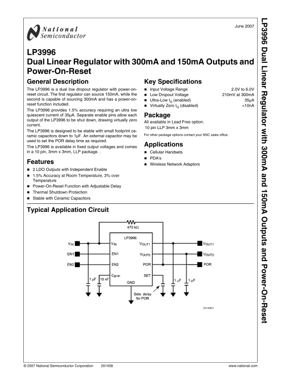
Typical Application Circuit
© 2007 National Semiconductor Corporation www.national.com
Page Summary Contents For NATIONAL SEMICONDUCTOR LP3996 User's Manual
Manual Details
| Brand | National |
|---|---|
| Pages | 18 |
| File Size | 508.79 KB |
| Published | June 01, 2026 |
Enter the captcha to get the download link:

Frequently Asked Questions
How can I set a delay time for the Power-On Reset (POR)?
Connect a capacitor between the SET pin and GND; if this is left open, there will be no POR delay.
What are the maximum current outputs available?
Regulator 1 provides 150mA max output, while Regulator 2 can source up to 300mA max output.
How do I minimize output noise and transient errors?
Connect a 10nF capacitor (BYP) from pin 4 to GND, and ensure standard 1µF capacitors are used at both OUT1 and OUT2.
Can the two regulator outputs be controlled independently?
Yes, separate enable pins (EN1 for Regulator 1 and EN2 for Regulator 2) allow each output to be individually switched on or off.