NATIONAL SEMICONDUCTOR ADC108S052 User's Manual
Summary
This highly reliable, low-power CMOS 10-bit Analog-to-Digital Converter features eight input channels and variable conversion rates up to 500 kSPS. Designed for demanding environments, it uses independent analog and digital supplies, ensuring optimal performance stability. This documentation provides comprehensive technical details, including electrical specifications, pinouts, and guidelines necessary for proper integration into applications such as automotive navigation systems, medical instruments, mobile communications gear, and industrial control systems.
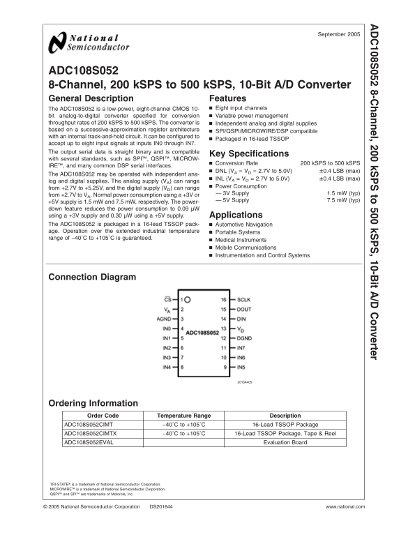
Page 1 Text Content
September
108S 8-C hannel,200 k S to k S ,10-B it /D onverter
ADC108S052 8-Channel, k SPS to k SPS, 10-Bit A/D Converter General Description Features
The ADC108S052 is low-power, eight-channel CMOS 10- Eight input channels bit analog-to-digital converter specified for conversion Variable power management
throughput rates of k SPS to k SPS. The converter is Independent analog and digital supplies based on successive-approximation register architecture
SPI/QSPI/MICROWIRE/DSP compatible
with an internal track-and-hold circuit. It can be configured to
Packaged in 16-lead TSSOP
accept up to eight input signals at inputs IN0 through IN7. The output serial data is straight binary and is compatible
Key Specifications
with several standards, such as SPI™, QSPI™, MICROW-
Conversion Rate k SPS to k SPS
IRE™, and many common DSP serial interfaces.
DNL (VA VD 2.7V to 5.0V) ±0.4 LSB (max)
The ADC108S052 may be operated with independent ana-
INL (VA VD 2.7V to 5.0V) ±0.4 LSB (max)
log and digital supplies. The analog supply (VA) can range
Power Consumption
from +2.7V to +5.25V, and the digital supply (VD) can range
3V Supply 1.5 m W (typ)
from +2.7V to VA. Normal power consumption using +3V or
5V Supply 7.5 m W (typ)
+5V supply is 1.5 m W and 7.5 m W, respectively. The power- down feature reduces the power consumption to 0.09 µW using +3V supply and 0.30 µW using +5V supply. Applications The ADC108S052 is packaged in 16-lead TSSOP pack- Automotive Navigation age. Operation over the extended industrial temperature Portable Systems range of −40˚C to +105˚C is guaranteed.
Medical Instruments Mobile Communications Instrumentation and Control Systems
Connection Diagram
Ordering Information
Order Code Temperature Range Description
ADC108S052CIMT −40˚C to +105˚C 16-Lead TSSOP Package ADC108S052CIMTX −40˚C to +105˚C 16-Lead TSSOP Package, Tape Reel ADC108S052EVAL Evaluation Board
TRI-STATE® is trademark of National Semiconductor Corporation. MICROWIRE™ is trademark of National Semiconductor Corporation. QSPI™ and SPI™ are trademarks of Motorola, Inc.
National Semiconductor Corporation DS201644 www.national.com
Page Summary Contents For NATIONAL SEMICONDUCTOR ADC108S052 User's Manual
Manual Details
| Brand | National |
|---|---|
| Pages | 17 |
| File Size | 843.81 KB |
| Published | June 02, 2026 |
Enter the captcha to get the download link:

Frequently Asked Questions
What type and placement of capacitors are required for the analog supply power pin?
The V+ power pin should be bypassed by a 1 µF and a 0.1 µF monolithic ceramic capacitor located within 1 cm.
How does a conversion reading begin using this chip?
A conversion process begins on the falling edge of the CS (Chip Select) pin, and continues as long as CS is held low.
What is the maximum guaranteed operating temperature range for the ADC108S052?
The guaranteed operating temperature range is from −40°C to +105°C.
How does the converter communicate its output data to the system?
The output serial data is straight binary and can be read out on the falling edges of the SCLK pin.