# A B C D E F G H I J K L M N O P Q R S T U V W X Y Z

National Semiconductor LM3691 Data Handbook Specifications Miniature 1A Step-Down DC-DC Converter for Portable Applications

Summary

The LM3691 is a miniature, high-accuracy step-down DC-DC converter designed to power ultra-low voltage circuits from single Li-Ion cells up to 1A. Operating reliably between 2.3V and 5.5V input ranges, the device features advanced ECO/PWM modes for exceptional efficiency and extended battery life in portable applications. This manual provides comprehensive details on its function, including application circuits, pin descriptions, micro SMD integration guidelines, and operational safety features. It is ideally suited for powering demanding low-voltage electronics like mobile phones, hand-held radios, and MP3 players.
📄 Preview 📖 Table of Contents Contents PAGE OF 18

Page 1 Text Content

ig ra , M in ia tu re , S te -D -D rte r fo r P rta le lic tio

June 11, 2008

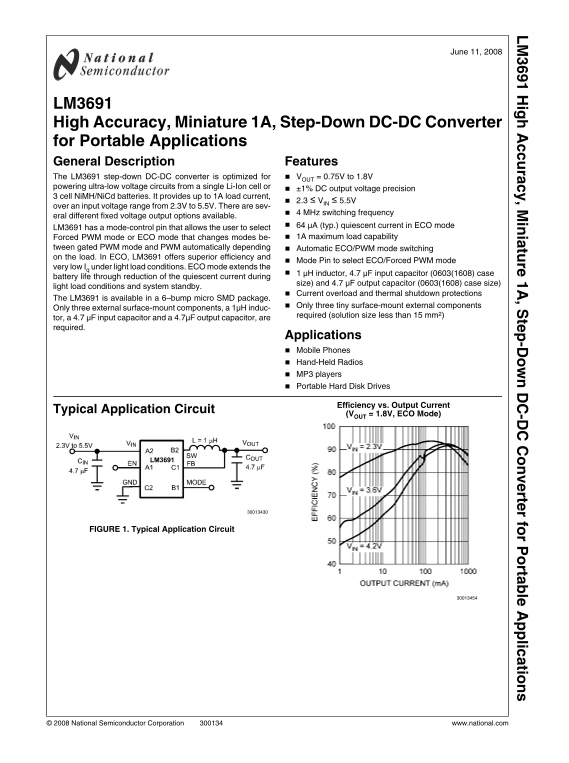
LM3691 High Accuracy, Miniature 1A, Step-Down DC-DC Converter for Portable Applications General Description Features The LM3691 step-down DC-DC converter is optimized for VOUT = 0.75V to 1.8V powering ultra-low voltage circuits from a single Li-Ion cell or

±1% DC output voltage precision

3 cell Ni MH/Ni Cd batteries. It provides up to 1A load current,

2.3 ≤ VIN ≤ 5.5V

over an input voltage range from 2.3V to 5.5V. There are sev-

4 MHz switching frequency

eral different fixed voltage output options available.

64 μA (typ.) quiescent current in ECO mode

LM3691 has a mode-control pin that allows the user to select

Forced PWM mode or ECO mode that changes modes be- 1A maximum load capability

tween gated PWM mode and PWM automatically depending Automatic ECO/PWM mode switching on the load. In ECO, LM3691 offers superior efficiency and

Mode Pin to select ECO/Forced PWM mode

very low Iq under light load conditions. ECO mode extends the

1 μH inductor, 4.7 μF input capacitor (0603(1608) case

battery life through reduction of the quiescent current during

size) and 4.7 μF output capacitor (0603(1608) case size)

light load conditions and system standby.

Current overload and thermal shutdown protections

The LM3691 is available in a 6–bump micro SMD package.

Only three tiny surface-mount external components

Only three external surface-mount components, a 1μH induc-

required (solution size less than 15 mm2)

tor, a 4.7 μF input capacitor and a 4.7μF output capacitor, are required.

Applications Mobile Phones Hand-Held Radios MP3 players Portable Hard Disk Drives

Efficiency vs. Output Current

Typical Application Circuit

(VOUT = 1.8V, ECO Mode)

FIGURE 1. Typical Application Circuit

© 2008 National Semiconductor Corporation www.national.com

Page Summary Contents For National Semiconductor LM3691 Data Handbook Specifications Miniature 1A Step-Down DC-DC Converter for Portable Applications

Page 1 ig ra , M in ia tu re , S te -D -D rte r fo r P rta le lic tio June 11, 2008 LM3691 High Accuracy, Miniature 1A, Step-Down DC-DC Converter for Portable Applications General Description Features The LM...
Page 2 Connection Diagram and Package Mark Information FIGURE 2. 6-Bump Thin Micro SMD Package, Large Bump NS Package Number TLA06LCA Note: The actual physical placement of the package marking will vary from...
Page 3 Ordering Information Order Number 6–bump Micro Voltage Option V Package Marking Supplied As 0.75 LM3691TL-0.75 250 units, Tape-and-Reel LM3691TLX–0.75 3000 units, Tape-and-Reel 0.85* LM3691TL-0.85 TBD...
Page 4 Absolute Maximum Ratings (Note 1) Operating Ratings (Notes 1, 2) If Military/Aerospace specified devices are required, Input Voltage Range 2.3V to 5.5V please contact the National Semiconductor Sales ...
Page 5 Block Diagram FIGURE 3. Simplified Functional Diagram www.national.com
Page 6 Typical Performance Characteristics LM3691TL Typical Application Circuit (page 1), VIN = 3.6V, VOUT = 1.8V, TA = 25°, L = 1.0 μH, 2520, (LQM2HP1R0), CIN = COUT = 4.7 μF, 0603(1608), 6.3V, (C1608X5R0J4...
Page 7 Output Voltage vs. Supply Voltage Output Voltage vs. Supply Voltage (VOUT = 0.75V) (VOUT = 1.8V) Output Voltage vs. Output Current Output Voltage vs. Output Current (VOUT = 0.75V) (VOUT = 1.8V) Input ...
Page 8 Efficiency vs. Output Current Efficiency vs. Output Current (VOUT = 0.75V, ECO Mode) (VOUT = 1.8V, ECO Mode) Efficiency vs. Output Current Efficiency vs. Output Current (VOUT = 0.75V, FPWM Mode) (VOUT...
Page 9 Output Voltage Ripple vs. Supply Voltage Output Voltage Ripple vs. Supply Voltage (VOUT = 0.75V) (VOUT = 1.8V) Closed Loop Current Limit vs. Temperature Closed Loop Current Limit vs. Temperature (VOUT...
Page 10 Load Transient Reponse Load Transient Reponse (VOUT = 0.75V, ECO Mode 1m A to 25 m A) (VOUT = 0.75V, ECO Mode 25 m A to 1m A) Load Transient Reponse Load Transient Reponse (VOUT = 1.8V, ECO Mode 1m A ...
Page 11 Load Transient Reponse Load Transient Reponse (VOUT = 1.8V, ECO Mode to PWM Mode) (VOUT = 1.8V, PWM Mode to ECO Mode) Load Transient Reponse Load Transient Reponse (VOUT = 0.75V, FPWM Mode) (VOUT = 0....
Page 12 Load Transient Reponse Load Transient Reponse (VOUT = 0.75V, PWM Mode) (VOUT = 1.8V, PWM Mode) Start Up into ECO Mode Start Up into PWM Mode (VOUT = 1.8V, ROUT = 1.8 kΩ) (VOUT = 1.8V, ROUT = 6 Ω) Star...
Page 13 Operation Description DEVICE INFORMATION The LM3691, a high-efficiency, step-down DC-DC switching buck converter, delivers a constant voltage from either a sin- gle Li-Ion or three cell Ni MH/Ni Cd ba...
Page 14 switch, reference, control and bias circuitry of the LM3691 are turned off. Setting EN high (>1.2V) enables normal operation. When turning on the device with EN soft-start is activated. EN pin shou...
Page 15 OUTPUT CAPACITOR SELECTION Application Information Use a 4.7μF, 6.3V ceramic capacitor, X7R, X5R or B types; INDUCTOR SELECTION do not use Y5V or F. DC bias voltage characteristics of ce- ramic capaci...
Page 16 corners. Initially, the trace to each pad should be 7 mil wide, MICRO SMD PACKAGE ASSEMBLY AND USE for a section approximately 7 mil long or longer, as a thermal Use of the Micro SMD package requires ...
Page 17 Physical Dimensions inches (millimeters) unless otherwise noted 6–bump Thin Micro SMD, Large Bump NS Package Number TLA06LCA X1 = 1.260mm ± 0.030mm X2 = 1.565mm ± 0.030mm X3 = 0.600mm ± 0.075mm www.na...
Page 18 ig ra in ia tu re te -D -D rt fo rt le li ti For more National Semiconductor product information and proven design tools, visit the following Web sites at: Products Design Support Amplifiers www.natio...

Manual Details

Brand National
Pages 18
File Size 2.15 MB
Published June 15, 2026
10 views

Enter the captcha to get the download link:

captcha

Frequently Asked Questions

What is the required input voltage range?

The recommended input voltage range (VIN) is 2.3V to 5.5V.

How can I save power in low-load situations?

Set the Mode Pin for ECO mode, which significantly reduces quiescent current and extends battery life during light load conditions.

What external components are needed for installation?

You only need three external surface-mount components: a 1μH inductor, a 4.7μF input capacitor, and a 4.7μF output capacitor.

How do I enable or disable the device?

The EN pin is enabled when voltage exceeds 1.2V and remains in shutdown mode if voltage drops below 0.4V.