NATIONAL SEMICONDUCTOR LM3687 Step-Down DC-DC Converter with Integrated Low Dropout Regulator and Startup Mode
Summary
The LM3687 is a high-efficiency step-down DC-DC converter tailored for complex, battery-powered portable electronics. Featuring integrated low dropout regulation and startup mode, it provides reliable dual power outputs across various voltage rails. This technical manual details the device's operational modes (PWM/PFM), connectivity diagrams, efficiency techniques, and specialized applications, ensuring engineers can design superior power management systems for products like mobile phones and PDAs while maximizing battery life.
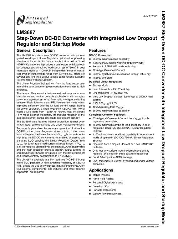
Page 1 Text Content
te -D -D rte r w ith In te ra te ro t R la to r a ta rtu
July 7, 2008
LM3687 Step-Down DC-DC Converter with Integrated Low Dropout Regulator and Startup Mode General Description Features The LM3687 is a step-down DC-DC converter with an inte- DC-DC Converter: grated low dropout Linear Regulator optimized for powering
750m A maximum load capability
ultra-low voltage circuits from a single Li-Ion cell or 3 cell
1.8MHz PWM fixed switching frequency (typ.)
Ni MH/Ni Cd batteries. It provides a dual output with fixed out-
Automatic PFM/PWM mode switching
put voltages and combined load current up to 750m A in post
regulation mode or 1100m A in independent mode of opera- 27µA typ. Quiescent Current
tion, over an input voltage range from 2.7V to 5.5V. There are Internal synchronous rectification for high efficiency several different fixed output voltage combinations available
Internal soft start
(refer to table 'Voltage Options').
Dual Rail Linear Regulator:
The Linear Regulator being driven from the fixed output volt-
Startup Mode
age of the buck converter (post regulation) translates to high
efficiency. Load transients < 25m Vpeak typ. The device offers superior features and performance for mo- Line transients < 1m Vpeak typ.
bile phones and similar portable applications with complex Very Low Dropout Voltage: 82m V typ. at 350m A load power management systems. Automatic intelligent switching current between PWM low-noise and PFM low-current mode offers
0.7V ≤ VIN_LIN ≤ 4.5V
improved efficiency over the full load current range. During
10µA typical IQ from VIN_LIN
full-power operation, a fixed-frequency 1.8MHz (typ.) PWM
350m A maximum load capability
mode drives loads from ~80m A to 750m A max. Hysteretic
PFM mode extends the battery life through reduction of the Combined Common Features:
quiescent current during light loads and system standby. 65µA typical Quiescent Current from VBATT if both
The LM3687 also features internal protection against over- regulators are enabled
temperature, current overload and under-voltage conditions. 750m A maximum combined load capability in post
Two enable pins allow the separate operation of either the regulation setup (DC-DC 400m A + Linear Regulator DC-DC or the Linear Regulator alone or both. If the power 350m A)
input voltage for the Linear Regulator VIN_LIN is not sufficiently 1100m A maximum total load capability in independent high (e.g. the DC-DC converter is not enabled or starting up) mode of operation (DC-DC: 750m A, Linear Regulator: a startup LDO supplies the Linear Regulator Output from 350m A) VBATT for 50m A rated load current (Startup Mode). If VIN_LIN Operates from a single Li-Ion cell or 3 cell Ni MH/Ni Cd is at the required voltage level, the startup LDO is deactivated batteries and the main regulator provides 350m A output current. In
Only four tiny surface-mount external components
shutdown mode (Enable pins pulled low) the device turns off
required (one inductor, three ceramic capacitors)
and reduces battery consumption to 0.1µA (typ.).
Small 9-bump micro SMD package
The LM3687 is available in a tiny, lead-free (NO PB) 9-bump
Over-temperature, current overload and under-voltage
micro SMD package. A high switching frequency of 1.8MHz
protection
(typ.) allows the use of tiny surface-mount components. Only four external components -one inductor and three ceramic
Applications
capacitors- are required.
Mobile Phones Hand-Held Radios Personal Digital Assistants Palm-top PCs Portable Instruments Battery Powered Devices
© 2008 National Semiconductor Corporation www.national.com
Page Summary Contents For NATIONAL SEMICONDUCTOR LM3687 Step-Down DC-DC Converter with Integrated Low Dropout Regulator and Startup Mode
Manual Details
| Brand | National |
|---|---|
| Pages | 22 |
| File Size | 627.48 KB |
| Published | June 04, 2026 |
Enter the captcha to get the download link:

Frequently Asked Questions
How does the LM3687 improve battery life during standby?
It features automatic PFM/PWM switching mode, which reduces quiescent current during light loads and system standby.
What built-in protections are included with this converter?
The device has internal protection against over-temperature, current overload, and under-voltage conditions.
How many external components does the LM3687 require for setup?
Only four tiny surface-mount external components—one inductor and three ceramic capacitors—are needed.
What is the maximum combined load capability?
It supports up to a 750mA maximum combined load capability in post regulation setup.