# A B C D E F G H I J K L M N O P Q R S T U V W X Y Z

National Semiconductor LM2734Z LM2734ZQ Thin SOT23 1A Load Step-Down DC-DC Regulator

Summary

The LM2734Z/LM2734ZQ is a high-efficiency, monolithic step-down DC-DC regulator designed for compact point-of-load conversion in portable and automotive electronics. This regulator provides stable 1A output current from input voltages spanning 3V to 20V within ultra-small thin SOT23 packages. The manual details the regulator’s advanced functions, including ultra-low standby current (30nA), precise regulation, and excellent thermal performance. It is ideal for electrical engineers designing battery-powered devices, USB systems, or automotive circuits requiring reliable power management in restricted space.
📄 Preview 📖 Table of Contents Contents PAGE OF 20

Page 1 Text Content

/L in te -D -D la to

June 12, 2008

LM2734Z/LM2734ZQ Thin SOT23 1A Load Step-Down DC-DC Regulator General Description Features The LM2734Z regulator is a monolithic, high frequency, PWM Thin SOT23-6 package, or 6 lead LLP package step-down DC/DC converter assembled in a 6-pin Thin

3.0V to 20V input voltage range

SOT23 and LLP non pull back package. It provides all the

0.8V to 18V output voltage range

active functions to provide local DC/DC conversion with fast

1A output current

transient response and accurate regulation in the smallest

possible PCB area. 3MHz switching frequency With a minimum of external components and online design 300mΩ NMOS switch

support through WEBENCH®™, the LM2734Z is easy to use. 30n A shutdown current The ability to drive 1A loads with an internal 300mΩ NMOS

0.8V, 2% internal voltage reference

switch using state-of-the-art 0.5µm Bi CMOS technology re-

Internal soft-start

sults in the best power density available. The world class

control circuitry allows for on-times as low as 13ns, thus sup- Current-Mode, PWM operation

porting exceptionally high frequency conversion over the en- Thermal shutdown tire 3V to 20V input operating range down to the minimum

LM2734ZQ is AEC-Q100 Grade 1 qualified and is

output voltage of 0.8V. Switching frequency is internally set

manufactured on an Automotive Grade Flow

to 3MHz, allowing the use of extremely small surface mount inductors and chip capacitors. Even though the operating fre-

Applications

quency is very high, efficiencies up to 85% are easy to

achieve. External shutdown is included, featuring an ultra-low DSL Modems

stand-by current of 30n A. The LM2734Z utilizes current-mode Local Point of Load Regulation control and internal compensation to provide high-perfor-

Battery Powered Devices

mance regulation over a wide range of operating conditions.

USB Powered Devices

Additional features include internal soft-start circuitry to re-

Automotive

duce inrush current, pulse-by-pulse current limit, thermal shutdown, and output over-voltage protection.

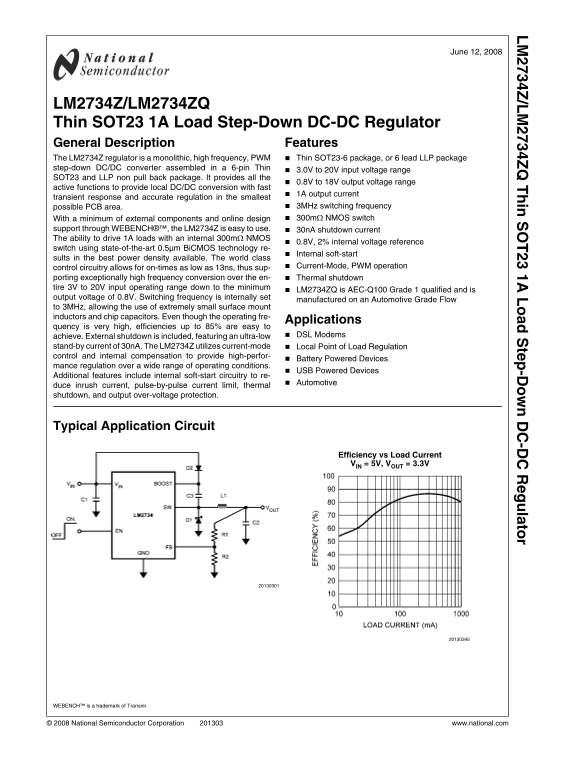
Typical Application Circuit

Efficiency vs Load Current VIN = 5V, VOUT = 3.3V

WEBENCH™ is a trademark of Transim.

© 2008 National Semiconductor Corporation www.national.com

Page Summary Contents For National Semiconductor LM2734Z LM2734ZQ Thin SOT23 1A Load Step-Down DC-DC Regulator

Page 1 /L in te -D -D la to June 12, 2008 LM2734Z/LM2734ZQ Thin SOT23 1A Load Step-Down DC-DC Regulator General Description Features The LM2734Z regulator is a monolithic, high frequency, PWM Thin SOT23-6 pa...
Page 2 Connection Diagrams 6-Lead TSOT 6-Lead LLP (3mm x 3mm) NS Package Number MK06A NS Package Number SDE06A Ordering Information Order Number Package Type NSC Package Package Supplied As Features Drawing ...
Page 3 Soldering Information Absolute Maximum Ratings (Note 1) Infrared/Convection Reflow (15sec) 220°C If Military/Aerospace specified devices are required, Wave Soldering Lead Temp. (10sec) 260°C please co...
Page 4 Typical Performance Characteristics All curves taken at VIN = 5V, VBOOST - VSW = 5V, L1 = 2.2 µH and TA = 25°C, unless specified otherwise. Efficiency vs Load Current Efficiency vs Load Current VOUT =...
Page 5 Block Diagram FIGURE 1. During the switch off-time, inductor current discharges Application Information through Schottky diode D1, which forces the SW pin to swing below ground by the forward voltage ...
Page 6 BOOST FUNCTION applied to the internal switch. In this circuit, CBOOST provides /L Capacitor CBOOST and diode D2 in Figure 3 are used to gen- a gate drive voltage that is slightly less than VOUT. erat...
Page 7 Design Guide INDUCTOR SELECTION The Duty Cycle (D) can be approximated quickly using the ratio of output voltage (VO) to input voltage (VIN): The catch diode (D1) forward voltage drop and the voltage ...
Page 8 Now that the ripple current or ripple ratio is determined, the transient is provided mainly by the output capacitor. The out- /L inductance is calculated by: put ripple of the converter is: where fs i...
Page 9 /L VSW is the voltage drop across the internal NFET when it is PCB Layout Considerations on, and is equal to: When planning layout there are a few things to consider when VSW = IOUT x RDSON trying to ...
Page 10 Design Example 1: Operating Conditions VIN 5.0V POUT 2.5W VOUT 2.5V PDIODE 151m W IOUT 1.0A PIND 75m W VD 0.35V PSWF 53m W Freq 3MHz PSWR 53m W IQ 1.5m A PCOND 187m W TRISE 8ns PQ 7.5m W TFALL 8ns PBO...
Page 11 Method 1: /L Design Example 3: To accurately measure the silicon temperature for a given Operating Conditions application, two methods can be used. The first method re- Package SOT23-6 quires the user...
Page 12 LLP Package Design Example 4: Operating Conditions The LM2734Z is packaged in a Thin SOT23-6 package and the 6–pin LLP. The LLP package has the same footprint as Package LLP-6 the Thin SOT23-6, but is...
Page 13 /L 3. Maximum junction temperature desired Package Selection 4. RθJA of the specific application, or RθJC (LLP or Thin To determine which package you should use for your specific SOT23-6) application,...
Page 14 LM2734Z Design Examples FIGURE 8. VBOOST Derived from VIN Operating Conditions: 5V to 1.5V/1A Bill of Materials for Figure 8 Part ID Part Value Part Number Manufacturer U1 1A Buck Regulator LM2734ZX N...
Page 15 FIGURE 9. VBOOST Derived from VOUT 12V to 3.3V/1A Bill of Materials for Figure 9 Part ID Part Value Part Number Manufacturer U1 1A Buck Regulator LM2734ZX National Semiconductor C1, Input Cap 10µF, 25...
Page 16 FIGURE 10. VBOOST Derived from VSHUNT 18V to 1.5V/1A Bill of Materials for Figure 10 Part ID Part Value Part Number Manufacturer U1 1A Buck Regulator LM2734ZX National Semiconductor C1, Input Cap 10µF...
Page 17 FIGURE 11. VBOOST Derived from Series Zener Diode (VIN) 15V to 1.5V/1A Bill of Materials for Figure 11 Part ID Part Value Part Number Manufacturer U1 1A Buck Regulator LM2734ZX National Semiconductor ...
Page 18 FIGURE 12. VBOOST Derived from Series Zener Diode (VOUT) 15V to 9V/1A Bill of Materials for Figure 12 Part ID Part Value Part Number Manufacturer U1 1A Buck Regulator LM2734ZX National Semiconductor C...
Page 19 Physical Dimensions inches (millimeters) unless otherwise noted 6-Lead SOT23 Package NS Package Number MK06A 6-Lead LLP Package NS Package Number SDE06A www.national.com
Page 20 /L in te -D -D la to Notes For more National Semiconductor product information and proven design tools, visit the following Web sites at: Products Design Support Amplifiers www.national.com/amplifiers...

Manual Details

Brand National
Pages 20
File Size 452.41 KB
Published June 17, 2026
5 views

Enter the captcha to get the download link:

captcha

Frequently Asked Questions

How do I set the desired output voltage?

Set it by connecting an external resistor divider to the FB (Feedback) pin.

What are the key protection features of this regulator?

It includes internal soft-start, thermal shutdown, pulse-by-pulse current limit, and over-voltage protection.

Is the device compatible with automotive applications?

Yes, the LM2734ZQ is AEC-Q100 Grade 1 qualified for use in automotive systems.

What is the acceptable input voltage range?

The operational input voltage range is specified as 3V to 20V.