National Semiconductor DS90CF563 DS90CF564 LVDS 18-Bit Color Flat Panel Display (FPD) Link — 65 MHz
Summary
This high-speed LVDS chipset pair provides an advanced interface solution for demanding flat panel display (FPD) applications. The transmitter and receiver are designed to convert high-bandwidth CMOS/TTL data into low Signal Electromagnetic Interference (low EMI), ultra-reliable LVDS signals up to 65 MHz, supporting speeds up to 171 Mbytes/s while significantly reducing cable size. This comprehensive manual details the electrical characteristics, operational parameters, and connectivity for integrating a robust display link across various graphics standards, making it essential for system engineers developing advanced LCD panel controllers.
Page 1 Text Content
查询DS90CF563供应商
90C F563/D 90C F564 LV 18-B it olor Flat anel D isplay (FP Link
DS90CF563/DS90CF564 LVDS 18-Bit Color Flat Panel Display (FPD) Link— MHz General Description Features
The DS90CF563 transmitter converts bits of CMOS/TTL to MHz shift clk support
data into three LVDS (Low Voltage Differential Signaling) Up to Mbytes/s bandwidth data streams. phase-locked transmit clock is transmitted in Cable size is reduced to save cost parallel with the data streams over fourth LVDS link. Every m V swing LVDS devices for low EMI cycle of the transmit clock bits of input data are sampled
Low power CMOS design m W typ)
and transmitted. The DS90CF564 receiver converts the
Power-down mode saves power 0.25 m W)
LVDS data streams into bits of CMOS/TTL data. At
PLL requires no external components
transmit clock frequency of MHz, bits of RGB data
Low profile 48-lead TSSOP package
and bits of LCD timing and control data (FPLINE,
FPFRAME, DRDY) are transmitted at rate of Mbps per Falling edge data strobe LVDS data channel. Using MHz clock, the data through- Compatible with TIA/EIA-644 LVDS standard
put is Mbytes per second. These devices are offered Single pixel per clock XGA (1024 768) with falling edge data strobes for convenient interface with Supports VGA, SVGA, XGA and higher variety of graphics and LCD panel controllers.
1.3 Gbps throughput
This chipset is an ideal means to solve EMI and cable size problems associated with wide, high speed TTL interfaces.
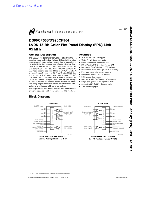
Block Diagrams
DS90CF563 DS90CF564
DS012615-2 DS012615-1
Order Number DS90CF563MTD Order Number DS90CF564MTD See NS Package Number MTD48 See NS Package Number MTD48
TRI-STATE® is registered trademark of National Semiconductor Corporation.
National Semiconductor Corporation DS012615 www.national.com
Page Summary Contents For National Semiconductor DS90CF563 DS90CF564 LVDS 18-Bit Color Flat Panel Display (FPD) Link — 65 MHz
Manual Details
| Brand | National |
|---|---|
| Pages | 12 |
| File Size | 290.54 KB |
| Published | June 05, 2026 |
Enter the captcha to get the download link:

Frequently Asked Questions
What types of graphics panels are compatible with this link?
It supports VGA, SVGA, XGA, and higher varieties of graphics and LCD panel controllers.
What is the maximum data throughput or bandwidth supported?
The device can handle up to 171 Mbytes/s bandwidth data streams, achieving a 1.3 Gbps throughput.
How does this chipset address issues with wide TTL interfaces?
It offers an ideal means to solve EMI and cable size problems associated with wide, high speed TTL interfaces.
What is the power consumption in standby mode?
The device includes a low power down-mode that saves power of less than 0.25 mW.