NATIONAL SEMICONDUCTOR DS25BR110 3.125 Gbps LVDS Buffer with Receive Equalization
Summary
Engineered for high-reliability data transfer, this product line features advanced single-channel buffers and receivers operating at 3.125 Gbps using LVDS signaling. Designed to maintain signal integrity over challenging media like lossy FR-4 backplanes, these ICs offer multiple levels of receive equalization and low jitter performance. This comprehensive manual details the technical specifications, operational parameters, and selection criteria for specialized buffers, repeaters, and drivers, making it essential for electronics engineers designing cutting-edge high-speed digital interconnect systems.
Page 1 Text Content
.1 ffe r w ith iv liza tio
November 6, 2007
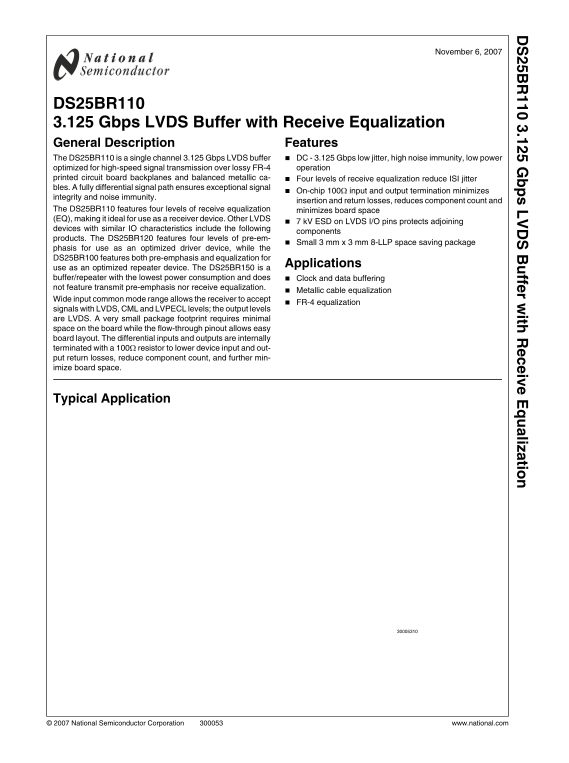
DS25BR110 3.125 Gbps LVDS Buffer with Receive Equalization General Description Features The DS25BR110 is a single channel 3.125 Gbps LVDS buffer DC - 3.125 Gbps low jitter, high noise immunity, low power optimized for high-speed signal transmission over lossy FR-4 operation printed circuit board backplanes and balanced metallic ca- Four levels of receive equalization reduce ISI jitter bles. A fully differential signal path ensures exceptional signal
On-chip 100Ω input and output termination minimizes
integrity and noise immunity.
insertion and return losses, reduces component count and
The DS25BR110 features four levels of receive equalization minimizes board space (EQ), making it ideal for use as a receiver device. Other LVDS
7 k V ESD on LVDS I/O pins protects adjoining
devices with similar IO characteristics include the following
components
products. The DS25BR120 features four levels of pre-em-
Small 3 mm x 3 mm 8-LLP space saving package
phasis for use as an optimized driver device, while the DS25BR100 features both pre-emphasis and equalization for
Applications
use as an optimized repeater device. The DS25BR150 is a buffer/repeater with the lowest power consumption and does Clock and data buffering not feature transmit pre-emphasis nor receive equalization.
Metallic cable equalization
Wide input common mode range allows the receiver to accept
FR-4 equalization
signals with LVDS, CML and LVPECL levels; the output levels are LVDS. A very small package footprint requires minimal space on the board while the flow-through pinout allows easy board layout. The differential inputs and outputs are internally terminated with a 100Ω resistor to lower device input and out- put return losses, reduce component count, and further min- imize board space.
Typical Application
© 2007 National Semiconductor Corporation www.national.com
Page Summary Contents For NATIONAL SEMICONDUCTOR DS25BR110 3.125 Gbps LVDS Buffer with Receive Equalization
Manual Details
| Brand | National |
|---|---|
| Pages | 16 |
| File Size | 437.14 KB |
| Published | May 30, 2026 |
Enter the captcha to get the download link:

Frequently Asked Questions
How do I adjust the received equalization level for optimal performance?
The EQ0 and EQ1 select pins allow adjustment of four levels: Off, Low, Medium, or High.
What types of materials is this buffer designed to handle signal transmission over?
It is optimized for high-speed signal transmission over lossy FR-4 printed circuit board backplanes and balanced metallic cables.
Are external termination resistors needed for the differential I/O pins?
No, the differential inputs and outputs are internally terminated with a 100Ω resistor to minimize board space.