National Semiconductor DS90CF581 DS90CF582 LVDS 24-Bit Color Flat Panel Display (FPD) Link Data Sheet
Summary
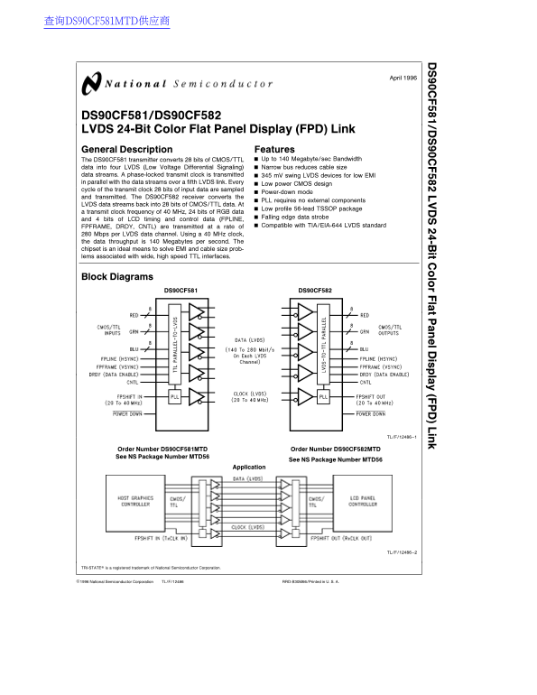
DS90CF581/DS90CF582 are high-performance integrated solutions designed for transmitting and receiving 24-Bit Color Flat Panel Display (FPD) links using low-voltage differential signaling (LVDS). This chipset supports blazing fast data transfer up to 140 MB/sec, effectively mitigating EMI challenges found in traditional wide signal interfaces. The comprehensive manual provides detailed electrical specifications, operational parameters, and application guidance needed for seamless integration of high-bandwidth video signals. It is essential tooling for hardware engineers developing professional display systems requiring reliable, low-power connectivity.
Page 1 Text Content
查询DS90CF581MTD供应商
April
-B it lo la is la (F in
DS90CF581/DS90CF582 LVDS 24-Bit Color Flat Panel Display (FPD) Link General Description Features
The DS90CF581 transmitter converts bits of CMOS/TTL Up to Megabyte/sec Bandwidth
data into four LVDS (Low Voltage Differential Signaling) Narrow bus reduces cable size data streams. phase-locked transmit clock is transmitted m V swing LVDS devices for low EMI in parallel with the data streams over fifth LVDS link. Every Low power CMOS design cycle of the transmit clock bits of input data are sampled
Power-down mode
and transmitted. The DS90CF582 receiver converts the
PLL requires no external components
LVDS data streams into bits of CMOS/TTL data. At
Low profile 56-lead TSSOP package
transmit clock frequency of MHz, bits of RGB data
Falling edge data strobe
and bits of LCD timing and control data (FPLINE,
FPFRAME, DRDY, CNTL) are transmitted at rate of Compatible with TIA/EIA-644 LVDS standard
Mbps per LVDS data channel. Using MHz clock, the data throughput is Megabytes per second. The chipset is an ideal means to solve EMI and cable size prob- lems associated with wide, high speed TTL interfaces.
Block Diagrams
DS90CF581 DS90CF582
TL/F/12486–1
Order Number DS90CF581MTD Order Number DS90CF582MTD See NS Package Number MTD56
See NS Package Number MTD56
Application
TL/F/12486–2
TRI-STATEÉ is registered trademark of National Semiconductor Corporation.
C1996 National Semiconductor Corporation TL/F/12486 RRD-B30M66/Printed in U. S. A.
Page Summary Contents For National Semiconductor DS90CF581 DS90CF582 LVDS 24-Bit Color Flat Panel Display (FPD) Link Data Sheet
Manual Details
| Brand | National |
|---|---|
| Pages | 12 |
| File Size | 213.91 KB |
| Published | June 15, 2026 |
Enter the captcha to get the download link:

Frequently Asked Questions
How fast is the data throughput possible with this link?
Using a 40 MHz clock, the data throughput can reach 140 Megabytes per second.
What standards does the DS90CF581/DS90CF582 comply with?
The device is compatible with the TIA/EIA-644 LVDS standard.
Can this chip be used in critical life support devices?
No, National's products are not authorized for use as critical components in life support systems without express written consent.
What are the roles of the transmitter and receiver chips?
The DS90CF581 transmits data to four LVDS links, while the DS90CF582 converts those LVDS streams back into CMOS/TTL data.