National Semiconductor DM5401 DM7401 Quad 2-Input NAND Gates with Open-Collector Outputs
Summary
This integrated circuit provides four independent 2-input NAND gates with open-collector outputs, requiring external pull-up resistors for optimal performance in digital logic systems. This technical manual offers hardware designers and electrical engineers comprehensive documentation, including detailed absolute maximum ratings, recommended operating conditions, and precise electrical characteristics. Use this guide to ensure reliable integration of the DM5401/DM7401 into your electronic circuit designs.
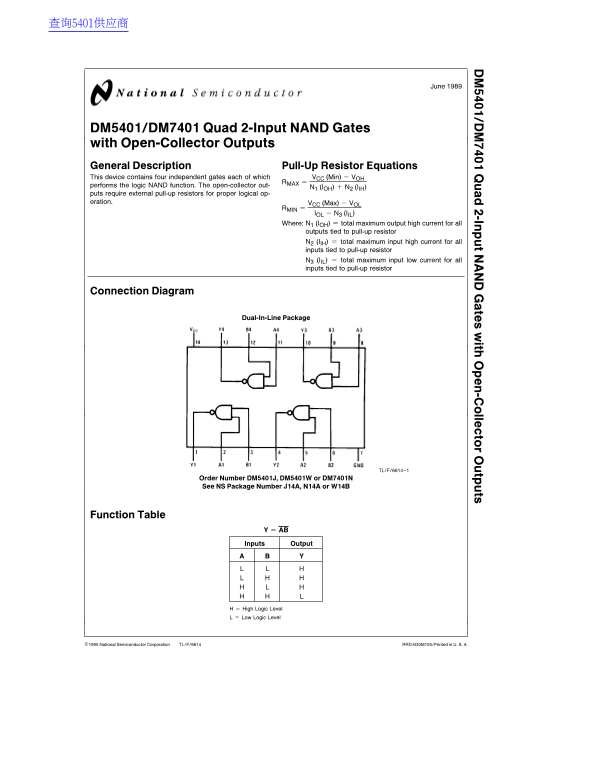
Page 1 Text Content
-In te ith -C lle to tp ts
DM5401/DM7401 Quad 2-Input NAND Gates with Open-Collector Outputs General Description Pull-Up Resistor Equations This device contains four independent gates each of which VCC (Min) VOH
performs the logic NAND function. The open-collector out- N1 (IOH) N2 (IIH) puts require external pull-up resistors for proper logical op- eration. VCC (Max) VOL
IOL N3 (IIL) Where: N1 (IOH) total maximum output high current for all outputs tied to pull-up resistor N2 (IIH) total maximum input high current for all inputs tied to pull-up resistor N3 (IIL) total maximum input low current for all inputs tied to pull-up resistor
Connection Diagram
Dual-In-Line Package
TL/F/6614–1
Order Number DM5401J, DM5401W or DM7401N See NS Package Number J14A, N14A or W14B
Function Table
Inputs Output
High Logic Level Low Logic Level
C1995 National Semiconductor Corporation TL/F/6614 RRD-B30M105/Printed in U. S. A.
Page Summary Contents For National Semiconductor DM5401 DM7401 Quad 2-Input NAND Gates with Open-Collector Outputs
Manual Details
| Brand | National |
|---|---|
| Pages | 4 |
| File Size | 98.34 KB |
| Published | May 29, 2026 |
Enter the captcha to get the download link:

Frequently Asked Questions
Are external resistors needed for proper operation of these gates?
Yes, the open-collector outputs require external pull-up resistors for proper logical operation.
What is the recommended supply voltage range (VCC) for this chip?
The optimal VCC voltage varies by part: 4.5V to 5.5V for DM5401 and 4.75V to 5.25V for DM7401.
Can I use this IC in life support devices or systems?
No, National Semiconductor warns that the product is not authorized for use as critical components in life support systems without express written approval.
What are the typical propagation delay times measured at 5V and 25°C?
The typical PLH delay time is 45 ns, and the PHL delay time is 15 ns.