National Semiconductor DM5417 DM7417 Hex Buffers with High Voltage Open-Collector Outputs
Summary
These hex buffers (DM5417/DM7417) provide robust signal conditioning with six independent gates and high voltage, open-collector outputs. This manual details the comprehensive electrical characteristics, operating ranges, and absolute maximum ratings required for proper system design. Ideal for electronic engineers needing reliable, buffered logic signals in various industrial or demanding applications where precise output control is essential.
Page 1 Text Content
查询DM5417供应商
ffe rs ith ig lta -C lle to tp ts
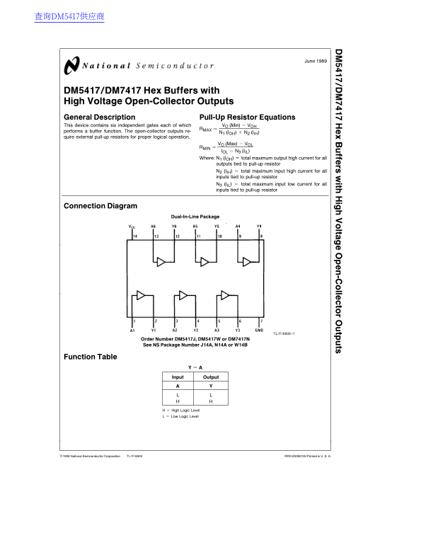
DM5417/DM7417 Hex Buffers with High Voltage Open-Collector Outputs General Description Pull-Up Resistor Equations This device contains six independent gates each of which VO (Min) VOH
performs buffer function. The open-collector outputs re- N1 (IOH) N2 (IIH) quire external pull-up resistors for proper logical operation.
VO (Max) VOL
IOL N3 (IIL) Where: N1 (IOH) total maximum output high current for all outputs tied to pull-up resistor N2 (IIH) total maximum input high current for all inputs tied to pull-up resistor N3 (IIL) total maximum input low current for all inputs tied to pull-up resistor
Connection Diagram
Dual-In-Line Package
TL/F/6505–1
Order Number DM5417J, DM5417W or DM7417N See NS Package Number J14A, N14A or W14B
Function Table
Input Output
High Logic Level Low Logic Level
C1995 National Semiconductor Corporation TL/F/6505 RRD-B30M105/Printed in U. S. A.
Page Summary Contents For National Semiconductor DM5417 DM7417 Hex Buffers with High Voltage Open-Collector Outputs
Manual Details
| Brand | National |
|---|---|
| Pages | 4 |
| File Size | 94.15 KB |
| Published | June 17, 2026 |
Enter the captcha to get the download link:

Frequently Asked Questions
What is required for proper logical operation of this device?
Since the open-collector outputs require external pull-up resistors.
How does the output voltage vary depending on the temperature range?
The recommended operating conditions table provides specific minimum and maximum voltages according to temperature ranges.
What are the key physical package options for the DM5417/DM7417?
Available packages include 14-Lead Ceramic Dual-In-Line (J), 14-Lead Molded Dual-In-Line (N), and 14-Lead Ceramic Flat Package (W).
What is the maximum current draw for the inputs?
Maximum input high current (IH) is specified as 2.4V at 40 mA, and low current (IL) is 0.8V at 1.6 mA.