# A B C D E F G H I J K L M N O P Q R S T U V W X Y Z

National Semiconductor DAC1006, DAC1007, DAC1008 - mP Compatible, Double-Buffered D/A Converters

Summary

Advanced multiply Digital-to-Analog Converters (DACs) designed for precision signal processing applications. These double-buffered components offer reliable conversion capability in 8-, 9-, and 10-bit resolutions, ideal for use in microprocessor-controlled systems, industrial instrumentation, or high-quality audio equipment. The manual provides detailed technical specifications covering electrical characteristics, package variants, operational parameters, and integration methods, essential for hardware designers and engineers building dedicated embedded solutions.
📄 Preview PAGE OF 22

Page 1 Text Content

查询DAC1006供应商

January

tib le

le -B ffe re to rte rs DAC1006/DAC1007/DAC1008 m P Compatible, Double-Buffered to Converters General Description Features

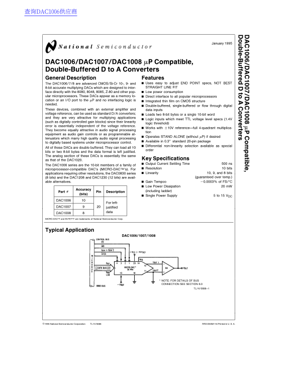
The DAC1006/7/8 are advanced CMOS/Si-Cr 10-, 9- and Uses easy to adjust END POINT specs, NOT BEST 8-bit accurate multiplying DACs which are designed to inter- STRAIGHT LINE FIT

face directly with the 8080, 8048, 8085, Z-80 and other pop- Low power consumption ular microprocessors. These DACs appear as memory lo- Direct interface to all popular microprocessors cation or an I/O port to the m P and no interfacing logic is

Integrated thin film on CMOS structure

needed.

Double-buffered, single-buffered or flow through digital

These devices, combined with an external amplifier and data inputs voltage reference, can be used as standard D/A converters;

Loads two 8-bit bytes or single 10-bit word

and they are very attractive for multiplying applications

Logic inputs which meet TTL voltage level specs (1.4V

(such as digitally controlled gain blocks) since their linearity

logic threshold)

error is essentially independent of the voltage reference.

Works with g10V referenceÐfull 4-quadrant multiplica-

They become equally attractive in audio signal processing

equipment as audio gain controls or as programmable at-

Operates STAND ALONE (without m P) if desired

tenuators which marry high quality audio signal processing

Available in 0.3× standard 20-pin package

to digitally based systems under microprocessor control.

Differential non-linearity selection available as special

All of these DACs are double buffered. They can load all

order

bits or two 8-bit bytes and the data format is justified. The analog section of these DACs is essentially the same

as that of the DAC1020. Key Specifications Output Current Settling Time ns

The DAC1006 series are the 10-bit members of family of

microprocessor-compatible DAC’s (MICRO-DACTM’s). For Resolution bits applications requiring other resolutions, the DAC0830 series Linearity 10, 9, and bits

(8 bits) and the DAC1208 and DAC1230 (12 bits) are avail- (guaranteed over temp.) able alternatives. Gain Tempco b0.0003% of FS/§C

Low Power Dissipation m W

Accuracy

Part Pin Description (including ladder)

(bits)

Single Power Supply to VDC

DAC1006

For left-

DAC1007 justified

DAC1008 MICRO-DACTM and BI-FETTM are trademarks of National Semiconductor Corp.

Typical Application

DAC1006/1007/1008

NOTE: FOR DETAILS OF BUS CONNECTION SEE SECTION 6.0

TL/H/5688–1

C1995 National Semiconductor Corporation TL/H/5688 RRD-B30M115/Printed in U. S. A.

Page Summary Contents For National Semiconductor DAC1006, DAC1007, DAC1008 - mP Compatible, Double-Buffered D/A Converters

Page 1 查询DAC1006供应商 January tib le le -B ffe re to rte rs DAC1006/DAC1007/DAC1008 m P Compatible, Double-Buffered to Converters General Description Features The DAC1006/7/8 are advanced CMOS/Si-Cr 10-, 9- an...
Page 2 Absolute Maximum Ratings (Notes 2) If Military/Aerospace specified devices are required, ESD Susceptibility (Note 11) 800V please contact the National Semiconductor Sales Lead Temp. (Soldering, second...
Page 3 Electrical Characteristics Tested at VCC 4.75 VDC and 15.75 VDC, TAe25§C, VREFe10.000 VDC unless otherwise noted (Continued) VCCe12VDCg5% See VCCe5VDCg5% Parameter Conditions to 15VDCg5% Units Min. Ty...
Page 4 Switching Waveforms TL/H/5688–2 Typical Performance Characteristics Errors vs. Supply Voltage Errors vs. Temperature Write Width, t W Control Setup Time, t CS Data Setup Time, t DS Data Hold Time, t D...
Page 5 Block and Connection Diagrams DAC1006/1007/1008 (20-Pin Parts) DAC1006/1007/1008 (20-Pin Parts) Dual-In-Line Package TL/H/5688–28 See Ordering Information USE DAC1006/1007/1008 FOR JUSTIFIED DATA TL/H...
Page 6 1.0 DEFINITION OF PACKAGE PINOUTS 1.1 Control Signals (All control signals are level actuated.) RFB: Feedback Resistor This is provided on the IC chip CS: Chip Select active low, it will enable WR. fo...
Page 7 Settling Time: Settling time is the time required from code 3.0 TTL COMPATIBLE LOGIC INPUTS transition until the DAC output reaches within g(/2 LSB of To guarantee TTL voltage compatibility of the log...
Page 8 4.2 Op Amp Bias Current Input Leads able ladder current to the IOUT1 output pin. These MOS The op amp bias current (IB) CAN CAUSE DC ERRORS. BI- switches operate in the current mode with small voltage...
Page 9 shown in Figure 4, where the sign of the reference voltage where VREF can be positive or negative and is the signed has been changed to provide positive output voltage. Note decimal equivalent of the ...
Page 10 5.2 Analog Operation in the Voltage Switching Mode Notice that this is unipolar operation since all voltages are positive. bipolar output voltage can be obtained by using Some useful application circu...
Page 11 FIGURE 10. Providing Bipolar Output Voltage with Single Op Amp TL/H/5688–13 FIGURE 11. Increasing the Output Voltage Swing The output voltage swing can be expanded by adding If the VOS is to be adjust...
Page 12 5.4.2 Current Switching with Bipolar Output Voltage 5.4.3 Voltage Switching with Unipolar Output Voltage The circuit of Figure shows the adjustments needed. Refer to the circuit of Figure and set all ...
Page 13 TL/H/5688-15 FIGURE 14. Voltage Switching with Bipolar Output Voltage 6.0 DIGITAL CONTROL DESCRIPTION The DAC1006 series of products can be used in wide 2) operating with double digital data buffer fo...
Page 14 These data possibilities are shown in Figure 15. Note that parts require the MS or Hi Byte data group to be transferred the justification of data depends on how the 10-bit data on the 1st write cycle....
Page 15 6.2.1 Automatic Transfer 6.2.3 Transfer Using an External Strobe This makes use of double byte (double precision) write. This is similar to the previous operation except the XFER The first byte (8 bit...
Page 16 TL/H/5688–21 FIGURE 17. Input Connections and Logic for DAC1006/1007/1008 with 16-Bit Data Bus Three operating modes are possible: flow through, single 6.4 Stand Alone Operation buffered, or double bu...
Page 17 7.0 MICROPROCESSOR INTERFACE The logic functions of the DAC1006 family have been ori- The circuit will perform an automatic transfer of the bits ented towards an ease of interface with all popular m P...
Page 18 the requirements of the DAC (with regard to justified PIA, and the LOW byte is loaded into ORB. The 10-bit data data) and the implementation of the PUSH instruction which transfer to the DAC and the c...
Page 19 NOTE: DATA HOLD TIME REDUCED TO THAT OF DM74LS374 (&10 ns) FIGURE 20. Isolating Data Bus from DAC Circuitry to Eliminate Digital Noise Coupling TL/H/5688–26 FIGURE 21. Digitally Controlled Amplifi...
Page 20 TL/H/5688–27 FIGURE 22. Digital to Synchro Converter Ordering Information For Justified Data 20-pin package. Temperature Range Accuracy 0§ to a70§C 0.05% (10-bit) DAC1006LCN DAC1006LCWM 0.10% (9-bit) ...
Page 21 Physical Dimensions inches (millimeters) Order Number DAC1006LCWM NS Package Number M20B
Page 22 ti le le -B ff re to rt rs Physical Dimensions inches (millimeters) (Continued) Order Number DAC1006LCN, DAC1007LCN or DAC1008LCN NS Package Number N20A LIFE SUPPORT POLICY NATIONAL’S PRODUCTS ARE NOT...

Manual Details

Brand National
Pages 22
File Size 372.10 KB
Published June 02, 2026
83 views

Enter the captcha to get the download link:

captcha

Frequently Asked Questions

What is the difference in resolution among the DAC1006, DAC1007, and DAC1008?

The DAC1006 offers 10 bits, the DAC1007 provides 9 bits, and the DAC1008 delivers 8 bits of resolution.

What are the recommended operational voltage ranges for these converters?

The devices can operate with a single power supply ranging from 5 V to 15 V DC.

How do these DACs interface with microprocessors?

They feature a direct interface designed for use with popular microprocessors like the 8080, 8048, and 8085.

Are these devices suitable for audio signal processing?

Yes, they can be used in audio signal processing equipment as high-quality audio gain controls or programmable attenuators.