# A B C D E F G H I J K L M N O P Q R S T U V W X Y Z

National Semiconductor ADC121S101 ADC101S101 ADC081S101 1MSPS, 12- 10- 8-Bit A D Converters in SOT-23 & LLP Owner's Manual & Specifications

Summary

These low-power CMOS Analog-to-Digital Converters (ADCs) provide high-resolution 12-, 10-, and 8-bit conversion up to 1 MSPS, ideal for demanding embedded systems. Designed with variable power management and compatibility across SPI/QSPI standards, they offer efficient operation down to under 5 µW during shutdown. The accompanying documentation provides detailed technical specifications, including package options (SOT-23 & LLP) and temperature ratings. Perfect for designers in medical devices, portable instrumentation, automotive navigation, and industrial control systems requiring reliable performance in variable environments.
📄 Preview PAGE OF 23

Page 1 Text Content

查询ADC081S101CIMF供应商

January

121S 101/A 101S 101/A 081S 1M ,12-/10-/8-B it /D onverters in T-23 LLP

ADC121S101/ADC101S101/ADC081S101 1MSPS, 12-/10-/8-Bit A/D Converters in SOT-23 LLP General Description Features

The ADC121S101, ADC101S101, and ADC081S101 are low Variable power management power, monolithic CMOS 12-, 10- and 8-bit analog-to-digital Packaged in 6-lead SOT-23 (ADC081S101 also converters that operate at MSPS. Each device is based on available in 6-Lead LLP package)

successive approximation register architecture with inter- Power supply used as reference nal track-and-hold. The serial interface is compatible with

Single +2.7V to +5.25V supply operation

several standards, such as SPI™, QSPI™, MICROWIRE™,

SPI™/QSPI™/MICROWIRE™/DSP compatible

and many common DSP serial interfaces. The ADC121S101/101S101/081S101 uses the supply volt-

Key Specifications

age as reference. This enables the devices to operate with

Resolution with no Missing Codes 12/10/8 bits

full-scale input range of to VDD. The conversion rate is

Conversion Rate MSPS

determined from the serial clock (SCLK) speed. These con-

verters offer shutdown mode, which can be used to trade DNL (ADC121S101) +0.5, -0.3 LSB (typ) throughput for power consumption. The ADC121S101/ INL (ADC121S101) 0.4 LSB (typ)

101S101/081S101 are operated with single supply that Power Consumption can range from +2.7V to +5.25V. Normal power consumption 3V Supply m W (typ) during continuous conversion, using +3V or +5V supply, is 5V Supply m W (typ) m W or m W, respectively. The power down feature, which is enabled by chip select (CS) pin, reduces the

Applications

power consumption to under µW using +5V supply. All

Automotive Navigation

three converters are available in 6-lead SOT-23 package,

FA/ATM Equipment

which provides an extremely small footprint for applications

where space is critical consideration. The ADC081S101 is Portable Systems also available in 6-lead LLP package. These products are Medical Instruments

designed for operation over the industrial temperature range Mobile Communications of −40˚C to +85˚C, with some parameters specified to

Instrumentation and Control Systems

+125˚C for the ADC121S101.

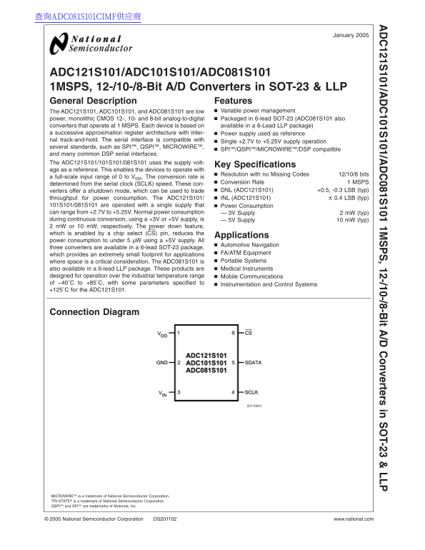
Connection Diagram

MICROWIRE™ is trademark of National Semiconductor Corporation. TRI-STATE® is trademark of National Semiconductor Corporation. QSPI™ and SPI™ are trademarks of Motorola, Inc.

National Semiconductor Corporation DS201102 www.national.com

Page Summary Contents For National Semiconductor ADC121S101 ADC101S101 ADC081S101 1MSPS, 12- 10- 8-Bit A D Converters in SOT-23 & LLP Owner's Manual & Specifications

Page 1 查询ADC081S101CIMF供应商 January 121S 101/A 101S 101/A 081S 1M ,12-/10-/8-B it /D onverters in T-23 LLP ADC121S101/ADC101S101/ADC081S101 1MSPS, 12-/10-/8-Bit A/D Converters in SOT-23 LLP General Descriptio...
Page 2 Ordering Information Order Code Temperature Description Mark Range ADC121S101CIMF −40˚C to 6-Lead SOT-23 Package X01C ADC101S101CIMF −40˚C to +85˚C 6-Lead SOT-23 Package X02C ADC081S101CIMF −40˚C to +...
Page 3 Absolute Maximum Ratings Operating Ratings (Note 2) 121S 101/A 101S 101/A 081S (Notes 1, 2) Operating Temperature Range If Military/Aerospace specified devices are required, ADC121S101 −40˚C TA +125˚C...
Page 4 ADC121S101 Converter Electrical Characteristics (Continued) The following specifications apply for VDD +2.7V to 5.25V, f SCLK MHz, f SAMPLE MSPS unless otherwise noted. Bold- face limits apply for TA ...
Page 5 ADC101S101 Converter Electrical Characteristics 121S 101/A 101S 101/A 081S The following specifications apply for VDD +2.7V to 5.25V, f SCLK MHz, f SAMPLE MSPS unless otherwise noted. Bold- face limit...
Page 6 ADC101S101 Converter Electrical Characteristics (Continued) The following specifications apply for VDD +2.7V to 5.25V, f SCLK MHz, f SAMPLE MSPS unless otherwise noted. Bold- face limits apply for TA ...
Page 7 ADC081S101 Converter Electrical Characteristics 121S 101/A 101S 101/A 081S The following specifications apply for VDD +2.7V to 5.25V, f SCLK MHz, f SAMPLE MSPS unless otherwise noted. Bold- face limit...
Page 8 ADC081S101 Converter Electrical Characteristics (Continued) The following specifications apply for VDD +2.7V to 5.25V, f SCLK MHz, f SAMPLE MSPS unless otherwise noted. Bold- face limits apply for TA ...
Page 9 ADC121S101/ADC101S101/ADC081S101 Timing Specifications 121S 101/A 101S 101/A 081S The following specifications apply for VDD +2.7V to 5.25V, f SCLK MHz, Boldface limits apply for TA −40˚C to +85˚C: al...
Page 10 OFFSET ERROR is the deviation of the first code transition Specification Definitions (000...000) to (000...001) from the ideal (i.e. GND 0.5 LSB APERTURE DELAY is the time after the falling edge of CS...
Page 11 Timing Diagrams 121S 101/A 101S 101/A 081S FIGURE 1. Timing Test Circuit FIGURE 2. ADC121S101 Serial Interface Timing Diagram FIGURE 3. ADC101S101 Serial Interface Timing Diagram www.national.com11
Page 12 Timing Diagrams (Continued) FIGURE 4. ADC081S101 Serial Interface Timing Diagram www.national.com
Page 13 Typical Performance Characteristics TA +25˚C, VDD 3V, f SAMPLE MSPS, f SCLK MHz, f IN 121S 101/A k Hz unless 101S otherwise 101/A stated. 081S ADC121S101 ADC121S101 DNL ADC121S101 INL ADC121S101 Spect...
Page 14 Typical Performance Characteristics TA +25˚C, VDD 3V, f SAMPLE MSPS, f SCLK MHz, f IN k Hz unless otherwise stated. (Continued) ADC121S101 SINAD vs. Input Frequency, k SPS ADC121S101 SINAD vs. Input F...
Page 15 Typical Performance Characteristics TA +25˚C, VDD 3V, f SAMPLE MSPS, f SCLK MHz, f IN 121S k Hz 101/A unless otherwise 101S 101/A stated. (Continued) 081S ADC101S101 DNL ADC101S101 INL ADC101S101 Spec...
Page 16 Typical Performance Characteristics TA +25˚C, VDD 3V, f SAMPLE MSPS, f SCLK MHz, f IN k Hz unless otherwise stated. (Continued) ADC081S101 DNL ADC081S101 INL ADC081S101 Spectral Response k Hz Input AD...
Page 17 Figure shows the device in hold mode: switch SW1 con- Applications Information nects the sampling capacitor to ground, maintaining the sampled voltage, and switch SW2 unbalances the compara- 1.0 ADC12...
Page 18 Applications Information cessive integer LSB values. The LSB widths for the (Continued) ADC121S101 is VDD 4096; for the ADC101S101 the LSB If CS goes low before the rising edge of SCLK, an additional ...
Page 19 Applications Information (Continued) 121S 101/A 101S 101/A 081S 4.0 SAMPLE CIRCUIT FIGURE 10. Equivalent Input Circuit 6.0 DIGITAL INPUTS AND OUTPUTS The ADC121S101/101S101/081S101 digital inputs (SCL...
Page 20 Applications Information tenth falling edges of SCLK, as shown in Figure 10. Once CS (Continued) has been brought high in this manner, the device will enter 9.0 SHUTDOWN MODE shutdown mode; the curren...
Page 21 Applications Information For example, to calculate the power consumption at (Continued) k SPS with VDD 5V, begin by calculating the fraction of time 121S 101/A 101S 101/A 081S spent in normal mode may...
Page 22 Physical Dimensions inches (millimeters) unless otherwise noted 6-Lead SOT-23 Order Number ADC121S101CIMF, ADC121S101CIMFX, ADC101S101CIMF, ADC101S101CIMFX, ADC081S101CIMF or ADC081S101CIMFX NS Packag...
Page 23 Notes 121S 101/A 101S 101/A 081S 1M ,12-/10-/8-B it /D onverters in T-23 LLP National does not assume any responsibility for use of any circuitry described, no circuit patent licenses are implied and ...

Manual Details

Brand National
Pages 23
File Size 897.31 KB
Published June 01, 2026
71 views

Enter the captcha to get the download link:

captcha

Frequently Asked Questions

What is the required power supply range and bypass method?

The devices require a quiet +2.7V to +5.25V source, which must be thoroughly bypassed with 0.1 µF and 1 µF capacitors proximate to the VDD pin.

How can I minimize power consumption during standby or low usage?

Use the shutdown mode for reduced throughput/power trade-off, or enable the power down feature via the CS pin to achieve less than 5 µW at +5V.

What serial communication protocols are supported by these converters?

They are compatible with several standards including SPI, QSPI, MICROWIRE, and various common DSP serial interfaces.