National Semiconductor 54F 74F20 Data Handbook
Summary
This dual 4-Input NAND Gate integrated circuit provides two independent gates, each executing the reliable NAND logic function for complex digital applications. The comprehensive manual details electrical characteristics, absolute maximum ratings, and diverse operational modes necessary for proper design integration. Suitable for electronics engineers and designers requiring high-performance logic components, it is available in multiple package types—including DIP, SOIC, and LCC carriers—to meet varying board constraints and military/aerospace grade standards.
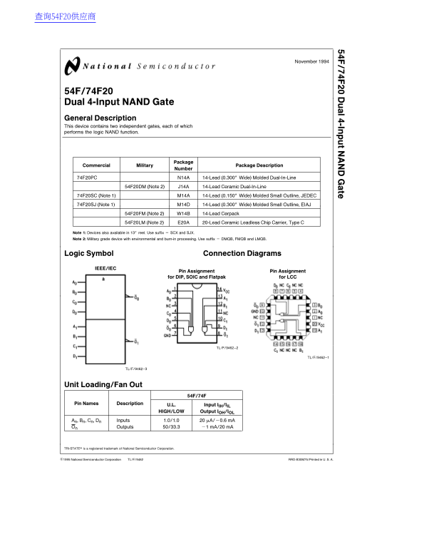
Page 1 Text Content
November
-In te
54F/74F20 Dual 4-Input NAND Gate General Description This device contains two independent gates, each of which performs the logic NAND function.
Package
Commercial Military Package Description
Number
74F20PC N14A 14-Lead (0.300× Wide) Molded Dual-In-Line
54F20DM (Note 2) J14A 14-Lead Ceramic Dual-In-Line
74F20SC (Note 1) M14A 14-Lead (0.150× Wide) Molded Small Outline, JEDEC
74F20SJ (Note 1) M14D 14-Lead (0.300× Wide) Molded Small Outline, EIAJ
54F20FM (Note 2) W14B 14-Lead Cerpack
54F20LM (Note 2) E20A 20-Lead Ceramic Leadless Chip Carrier, Type
Note 1: Devices also available in 13× reel. Use suffix SCX and SJX. Note 2: Military grade device with environmental and burn-in processing. Use suffix DMQB, FMQB and LMQB.
Logic Symbol Connection Diagrams
IEEE/IEC
Pin Assignment Pin Assignment for DIP, SOIC and Flatpak for LCC
TL/F/9462–2
TL/F/9462–1
TL/F/9462–3
Unit Loading/Fan Out
Pin Names Description U.L. Input IIH/IIL
HIGH/LOW Output IOH/IOL
An, Bn, Cn, Dn Inputs 1.0/1.0 m A/b0.6 m A
On Outputs 50/33.3 b1 m A/20 m A
TRI-STATEÉ is registered trademark of National Semiconductor Corporation.
C1995 National Semiconductor Corporation TL/F/9462 RRD-B30M75/Printed in U. S. A.
Page Summary Contents For National Semiconductor 54F 74F20 Data Handbook
Manual Details
| Brand | National |
|---|---|
| Pages | 6 |
| File Size | 140.80 KB |
| Published | June 04, 2026 |
Enter the captcha to get the download link:

Frequently Asked Questions
What is the recommended operating temperature range for military devices?
The specified operating temperatures for Military grade components are from -55°C to 125°C.
How do I select a small outline package version of the chip?
Small Outline packages are available in both SOIC JEDEC and EIAJ formats.
What is the recognized voltage level for an input HIGH signal?
The minimum required Input HIGH Voltage ($ ext{V}_{ ext{IH}}$) is 2.0 V.
What is the low-side current limitation when operating at 5.0V?
The specified Output LOW Current (Min $ ext{I}_{ ext{OL}}$) is 20 mA.