National Semiconductor - FPD87352CXA Data Handbook/Manual
Summary
This advanced timing controller is engineered specifically for high-definition flat panel displays, including monitors and HDTVs. Functioning as a centralized solution, it manages video data conversion using low-power LVDS and robust RSDS outputs. Integrated features like Response Time Compensation (RTC) significantly improve the visual fidelity of fast-moving images, while support for XGA, WXGA, and HDTV standards ensures broad compatibility. It is essential hardware for display manufacturers requiring reliable, high-performance signal generation in modern panel electronics.
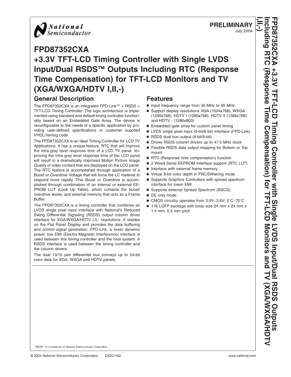
Page 1 Text Content
FP 87352C +3.3V TFT-LC Tim ing ontroller ith ingle LV Input/D ual R utputs Including TC (R esponse Tim om pensation) for TFT-LC PRELIMINARY onitors and TV (X /W /H TV
I,II,-) July
FPD87352CXA +3.3V TFT-LCD Timing Controller with Single LVDS Input/Dual RSDS™ Outputs Including RTC (Response Time Compensation) for TFT-LCD Monitors and TV (XGA/WXGA/HDTV I,II,-) General Description Features
The FPD87352CXA is an integrated FPD-Link™ RSDS Input frequency range from MHz to MHz TFT-LCD Timing Controller. The logic architecture is imple- Support display resolutions XGA (1024x768), WXGA mented using standard and default timing controller function- (1280x768), HDTV (1280x768), HDTV II (1366x768) ality based on an Embedded Gate Array. The device is and HDTV (1280x800)
reconfigurable to the needs of specific application by pro- Embedded gate array for custom panel timing viding user-defined specifications or customer supplied
LVDS single pixel input (8-bit/6-bit) interface (FPD-Link)
VHDL/Verilog code.
RSDS dual bus output (8-bit/6-bit)
The FPD87352CXA is an ideal Timing Controller for LCD TV
Drives RSDS column drivers up to 47.5 MHz clock
Applications. It has unique feature, RTC that will improve
Flexible RSDS data output mapping for or
the intra-gray level response time of LCD TV panel. Im-
mount
proving the intra-gray level response time of the LCD panel
RTC (Response time compensation) function
will result in dramatically improved Motion Picture Image
Wired Serial EEPROM Interface support (RTC LUT)
Quality of video content that are displayed on the LCD panel.
Interface with external frame memory
The RTC feature is accomplished through application of
Boost or Overdrive Voltage that will force the LC material to Virtual 8-bit color depth in FRC/Dithering mode respond more rapidly. This Boost or Overdrive is accom- Supports Graphics Controllers with spread spectrum plished through combination of an internal or external EE- interface for lower EMI
PROM LUT (Look Up Table), which contains the boost/ Supports external Spread Spectrum (SSCG) overdrive levels, and external memory that acts as Frame DE only mode Buffer.
CMOS circuitry operates from 3.0V–3.6V; 0˚C–70˚C
The FPD87352CXA is timing controller that combines an LQFP package with body size mm mm LVDS single pixel input interface with National’s Reduced 1.4 mm, 0.5 mm pitch Swing Differential Signaling (RSDS) output column driver interface for XGA/WXGA/HDTV I,II,- resolutions. It resides on the Flat Panel Display and provides the data buffering and control signal generation. FPD-Link, lower dynamic power, low EMI (Electro Magnetic Interference) interface is used between this timing controller and the host system. RSDS interface is used between the timing controller and the column drivers. The dual 13/10 pair differential bus conveys up to 24-bit color data for XGA, WXGA and HDTV panels.
RSDS™ is trademark of National Semiconductor Corporation.
National Semiconductor Corporation DS201162 www.national.com
Page Summary Contents For National Semiconductor - FPD87352CXA Data Handbook/Manual
Manual Details
| Brand | National |
|---|---|
| Pages | 5 |
| File Size | 132.93 KB |
| Published | June 06, 2026 |
Enter the captcha to get the download link:

Frequently Asked Questions
What display resolutions are supported by the FPD87352CXA?
It supports XGA (1024x768), WXGA, HDTV I (1280x768), and HDTV II (1366x768).
What is the function of the RTC feature?
RTC (Response Time Compensation) improves the intra-gray level response time of the LCD panel by adjusting grey values.
Which input interface is used for connection to the host system?
It uses a single LVDS pixel input interface, known as FPD-Link, which minimizes EMI and dynamic power.
What are the operating temperature and voltage requirements?
The CMOS circuitry operates from 3.0V–3.6V across a temperature range of 0˚C to 70˚C.