National Semiconductor 54174 DM54174 DM74174, 54175 DM54175 DM74175 - Hex Quad D Flip-Flops with Clear Data Sheet Manual
Summary
These reliable D Flip-Flops are fundamental TTL digital building blocks designed for storing data within electronic circuits. Available in Hex and Quad configurations, they feature positive-edge triggering and dedicated clear inputs, ensuring precise data handling. The manual provides comprehensive technical specifications, including detailed electrical characteristics, timing diagrams, application guidance, and ordering information. Ideal for electronics engineers and circuit designers integrating reliable storage registers into digital systems.
Page 1 Text Content
lip -F lo ith le
54174/DM54174/DM74174, 54175/DM54175/DM74175 Hex/Quad Flip-Flops with Clear General Description Features
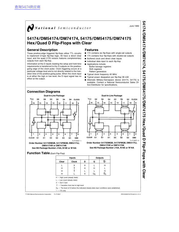
These positive-edge triggered flip-flops utilize TTL circuitry contains six flip-flops with single-rail outputs
to implement D-type flip-flop logic. All have direct clear contains four flip-flops with double-rail outputs input, and the quad (175) version features complementary Buffered clock and direct clear inputs outputs from each flip-flop. Individual data input to each flip-flop Information at the inputs meeting the setup and hold time Applications include: requirements is transferred to the outputs on the positive- Buffer/storage registers going edge of the clock pulse. Clock triggering occurs at Shift registers particular voltage level and is not directly related to the tran- Pattern generators sition time of the positive-going pulse. When the clock input
Typical clock frequency MHz
is at either the high or low level, the input signal has no
Typical power dissipation per flip-flop m W
effect at the output.
Alternate Military/Aerospace device (54174, 54175) is available. Contact National Semiconductor Sales Of- fice/Distributor for specifications.
Connection Diagrams
Dual-In-Line Package Dual-In-Line Package
TL/F/6557–1 TL/F/6557–2
Order Number 54174DMQB, 54174FMQB, DM54174J, Order Number 54175DMQB, 54175FMQB, DM54175J,
DM54174W or DM74174N DM54175W or DM74175N
See NS Package Number J16A, N16E or W16A See NS Package Number J16A, N16E or W16A
Function Table (Each Flip-Flop)
Inputs Outputs
Clear Clock Q²
High Level (steady state) Low Level (steady state) Don’t Care Transition from low to high level Q0 The level of before the indicated steady-state input conditions were established. only
C1995 National Semiconductor Corporation TL/F/6557 RRD-B30M105/Printed in U. S. A.
Page Summary Contents For National Semiconductor 54174 DM54174 DM74174, 54175 DM54175 DM74175 - Hex Quad D Flip-Flops with Clear Data Sheet Manual
Manual Details
| Brand | National |
|---|---|
| Pages | 8 |
| File Size | 151.11 KB |
| Published | June 16, 2026 |
Enter the captcha to get the download link:

Frequently Asked Questions
What are the differences between the '174 and '175 models?
The '174 has single-rail outputs (six flip-flops), while the '175 has double-rail outputs (four flip-flops).
What is the typical clock frequency for these flip-flops?
The typical clock frequency is 40 MHz.
Are military or aerospace versions available?
Yes, alternate Military/Aerospace devices (54174, 54175) are available; contact a distributor for details.
What power supply voltage range should be used?
The typical operating supply voltage varies between 4.5V and 5.5V (Nominal 5V).
How much time is required to set the data input (Setup Time)?
The minimum data setup time ($t_{SU}$) is 20 ns.