National LP3944 Data Sheet Manual
Summary
The LP3944 is an integrated LED driver chip designed for controlling up to eight individual LEDs with RGB/White/Blue capabilities. This manual provides comprehensive technical details, including the pinout, electrical characteristics, and operating specifications required for implementation. It is ideal for embedded system designers working on consumer electronics such as smart toys, indicator lights, or digital cameras that require precise, variable dimming and color control using an I²C interface.
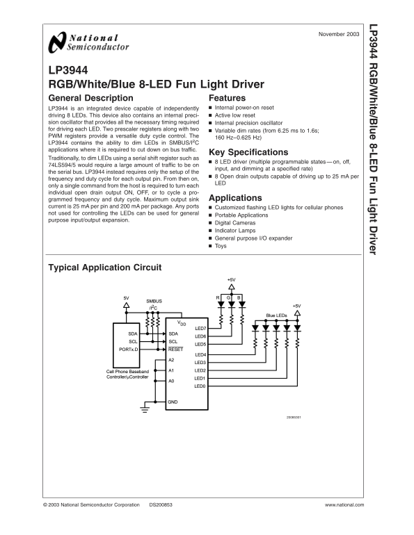
Page 1 Text Content
November
LP /W hite/B lue 8-LE Fun Light river
LP3944 RGB/White/Blue 8-LED Fun Light Driver General Description Features
LP3944 is an integrated device capable of independently Internal power-on reset driving LEDs. This device also contains an internal preci- Active low reset
sion oscillator that provides all the necessary timing required Internal precision oscillator for driving each LED. Two prescaler registers along with two
Variable dim rates (from 6.25 ms to 1.6s;
PWM registers provide versatile duty cycle control. The
Hz–0.625 Hz)
LP3944 contains the ability to dim LEDs in SMBUS/I2C applications where it is required to cut down on bus traffic.
Key Specifications
Traditionally, to dim LEDs using serial shift register such as
LED driver (multiple programmable states on, off,
74LS594/5 would require large amount of traffic to be on
input, and dimming at specified rate)
the serial bus. LP3944 instead requires only the setup of the
Open drain outputs capable of driving up to m A per
frequency and duty cycle for each output pin. From then on,
only single command from the host is required to turn each individual open drain output ON, OFF, or to cycle pro-
grammed frequency and duty cycle. Maximum output sink Applications
current is m A per pin and m A per package. Any ports Customized flashing LED lights for cellular phones not used for controlling the LEDs can be used for general
Portable Applications
purpose input/output expansion.
Digital Cameras Indicator Lamps General purpose I/O expander Toys
Typical Application Circuit
National Semiconductor Corporation DS200853 www.national.com
Page Summary Contents For National LP3944 Data Sheet Manual
Manual Details
| Brand | National |
|---|---|
| Pages | 12 |
| File Size | 249.63 KB |
| Published | May 29, 2026 |
Enter the captcha to get the download link:

Frequently Asked Questions
What is the maximum current sink per LED pin?
The device can sink up to 25 mA per individual open drain output pin.
What is the safe operating voltage range for the chip?
The recommended supply voltage (Vdd) operates within a range of 2.3V to 5.5V.
Can this component be used in life support systems?
No, the manufacturer states that its products are not authorized for use as critical components in life support devices without express written approval.
How does the LP3944 control dimming rates?
It uses two prescaler registers and PWM registers to provide general duty cycle control, ranging from 6.25 ms to 1.6s.