National LM5111 Data Sheet / Manual
Summary
The LM5111 is a high-performance dual compound gate driver designed for robust power applications, including switch-mode power supplies and motor/solenoid control. Featuring advanced MOSFET driving capabilities with 5A peak sink current and integrated UVLO protection, it significantly improves efficiency over standard drivers. This comprehensive guide provides detailed technical specifications, operational parameters (including TTL compatibility), pin descriptions, and ordering information essential for electrical engineers designing high-current power electronics systems.
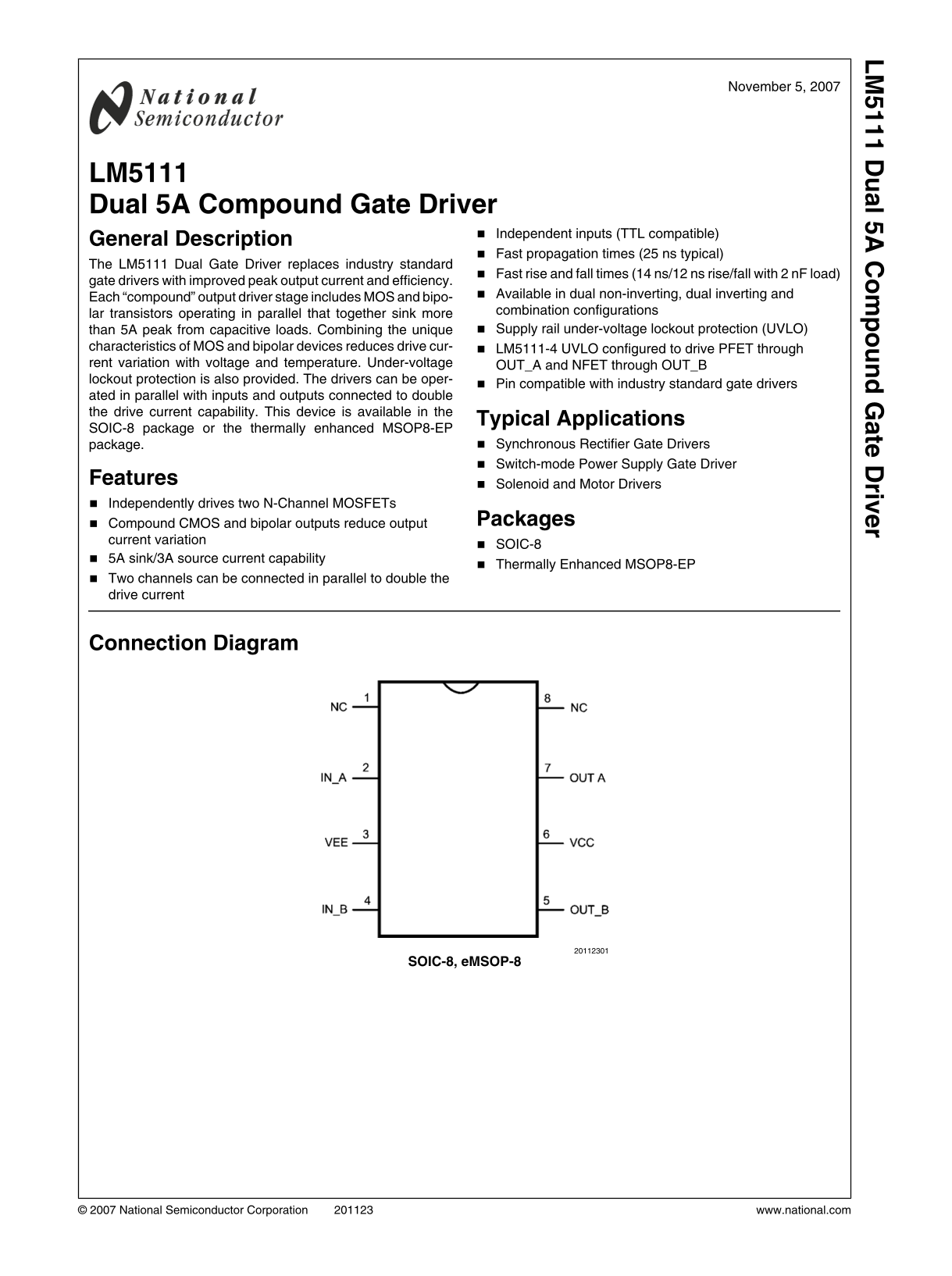
Page 1 Text Content
l 5 te riv
November 5, 2007
LM5111 Dual 5A Compound Gate Driver
Independent inputs (TTL compatible)
General Description
Fast propagation times (25 ns typical)
The LM5111 Dual Gate Driver replaces industry standard
Fast rise and fall times (14 ns/12 ns rise/fall with 2 n F load)
gate drivers with improved peak output current and efficiency.
Each “compound” output driver stage includes MOS and bipo- Available in dual non-inverting, dual inverting and lar transistors operating in parallel that together sink more combination configurations than 5A peak from capacitive loads. Combining the unique Supply rail under-voltage lockout protection (UVLO)
characteristics of MOS and bipolar devices reduces drive cur- LM5111-4 UVLO configured to drive PFET through rent variation with voltage and temperature. Under-voltage OUT_A and NFET through OUT_B lockout protection is also provided. The drivers can be oper-
Pin compatible with industry standard gate drivers
ated in parallel with inputs and outputs connected to double the drive current capability. This device is available in the
Typical Applications
SOIC-8 package or the thermally enhanced MSOP8-EP
package. Synchronous Rectifier Gate Drivers Switch-mode Power Supply Gate Driver
Features
Solenoid and Motor Drivers
Independently drives two N-Channel MOSFETs
Compound CMOS and bipolar outputs reduce output Packages
current variation
SOIC-8
5A sink/3A source current capability
Thermally Enhanced MSOP8-EP
Two channels can be connected in parallel to double the drive current
Connection Diagram
SOIC-8, e MSOP-8
© 2007 National Semiconductor Corporation www.national.com
Page Summary Contents For National LM5111 Data Sheet / Manual
Manual Details
| Brand | National |
|---|---|
| Pages | 12 |
| File Size | 289.95 KB |
| Published | July 22, 2026 |
Enter the captcha to get the download link:

Frequently Asked Questions
What is the current output capability of the drivers?
Each output stage can source 3A and sink 5A.
How can I increase the overall drive current?
Two channels can be connected in parallel to double the drive current capability.
What are the package options for this device?
It is available in SOIC-8 or thermally enhanced MSOP8-EP packages.
Does it have built-in protection features?
Yes, it includes Supply rail UVLO and under-voltage lockout protection for OUT_A and OUT_B.