National DS90C031B Data Sheet/Manual
Summary
The DS90C031B is a high-performance quad CMOS differential line driver engineered for reliable, ultra-low power data transmission in high-speed point-to-point applications. This device supports LVDS signaling at speeds exceeding 155 Mbps while accepting standard TTL/CMOS inputs. The accompanying documentation provides comprehensive technical specifications, electrical characteristics, and functional guides necessary for system designers integrating advanced, fail-safe communication interfaces into their circuits.
Page 1 Text Content
查询DS90C031B供应商
90C 031B LV uad ifferential Line river
March
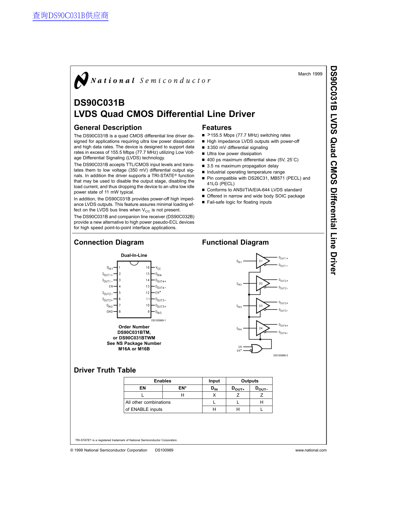
DS90C031B LVDS Quad CMOS Differential Line Driver General Description Features
The DS90C031B is quad CMOS differential line driver de- >155.5 Mbps (77.7 MHz) switching rates
signed for applications requiring ultra low power dissipation High impedance LVDS outputs with power-off and high data rates. The device is designed to support data ±350 m V differential signaling rates in excess of 155.5 Mbps (77.7 MHz) utilizing Low Volt- Ultra low power dissipation age Differential Signaling (LVDS) technology.
ps maximum differential skew (5V, 25˚C)
The DS90C031B accepts TTL/CMOS input levels and trans- 3.5 ns maximum propagation delay lates them to low voltage (350 m V) differential output sig-
Industrial operating temperature range
nals. In addition the driver supports TRI-STATE® function
Pin compatible with DS26C31, MB571 (PECL) and
that may be used to disable the output stage, disabling the
41LG (PECL)
load current, and thus dropping the device to an ultra low idle
Conforms to ANSI/TIA/EIA-644 LVDS standard
power state of m W typical.
Offered in narrow and wide body SOIC package
In addition, the DS90C031B provides power-off high imped-
Fail-safe logic for floating inputs
ance LVDS outputs. This feature assures minimal loading ef- fect on the LVDS bus lines when VCC is not present. The DS90C031B and companion line receiver (DS90C032B) provide new alternative to high power pseudo-ECL devices for high speed point-to-point interface applications.
Connection Diagram Functional Diagram
Dual-In-Line
DS100989-1
Order Number DS90C031BTM, or DS90C031BTWM See NS Package Number M16A or M16B
DS100989-2
Driver Truth Table
Enables Input Outputs EN EN* DIN DOUT+ DOUT−
All other combinations of ENABLE inputs
TRI-STATE® is registered trademark of National Semiconductor Corporation.
National Semiconductor Corporation DS100989 www.national.com
Page Summary Contents For National DS90C031B Data Sheet/Manual
Manual Details
| Brand | National |
|---|---|
| Pages | 12 |
| File Size | 256.04 KB |
| Published | July 22, 2026 |
Enter the captcha to get the download link:

Frequently Asked Questions
What is the maximum data rate this driver supports?
The device supports differential signaling rates in excess of 155.5 Mbps.
How does it handle low power or idle states?
It features a TRI-STATE function and power-off high impedance to minimize bus loading effect.
Can I use this component as part of life support equipment?
No, use is prohibited in life support devices without express written approval from the manufacturer.