National DS90C032 Data Sheet
Summary
This ultra low power quad CMOS differential line receiver is engineered for high-speed point-to-point applications requiring robust reception of LVDS signals up to 155.5 Mbps. The device accepts small swing, low voltage differential inputs and converts them into TTL-compatible CMOS outputs, minimizing power dissipation compared to traditional devices. The accompanying documentation provides comprehensive technical details on electrical characteristics, operating ratings (including military specifications), performance curves, timing diagrams, and industry compatibility standards, making it essential for engineers designing advanced digital interface systems.
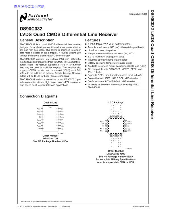
Page 1 Text Content
查询DS90C032供应商
September
90C LV uad ifferential Line eceiver
DS90C032 LVDS Quad CMOS Differential Line Receiver General Description Features
The DS90C032 is quad CMOS differential line receiver >155.5 Mbps (77.7 MHz) switching rates designed for applications requiring ultra low power dissipa- Accepts small swing (350 m V) differential signal levels
tion and high data rates. The device is designed to support Ultra low power dissipation data rates in excess of 155.5 Mbps (77.7 MHz) utilizing Low
ps maximum differential skew (5V, 25˚C)
Voltage Differential Signaling (LVDS) technology.
6.0 ns maximum propagation delay
The DS90C032 accepts low voltage (350 m V) differential
Industrial operating temperature range
input signals and translates them to CMOS (TTL compatible)
Military operating temperature range option
output levels. The receiver supports TRI-STATE® function
Available in surface mount packaging (SOIC) and (LCC)
that may be used to multiplex outputs. The receiver also
Pin compatible with DS26C32A, MB570 (PECL) and
supports OPEN, shorted and terminated (100Ω) input Fail-
41LF (PECL)
safe with the addition of external failsafe biasing. Receiver
Supports OPEN, short and terminated input fail-safe
output will be HIGH for both Failsafe conditions.
Compatible with IEEE 1596.3 SCI LVDS standard
The DS90C032 and companion line driver (DS90C031) pro-
Conforms to ANSI/TIA/EIA-644 LVDS standard
vide new alternative to high power psuedo-ECL devices for
high speed point-to-point interface applications. Available to Standard Microcircuit Drawing (SMD) 5962-95834
Connection Diagrams
Dual-In-Line LCC Package
Order Number DS90C032TM
See NS Package Number M16A
Order Number DS90C032E-QML
See NS Package Number E20A For complete Military Specifications, refer to appropriate SMD or MDS.
TRI-STATE® is registered trademark of National Semiconductor Corporation.
National Semiconductor Corporation DS011945 www.national.com
Page Summary Contents For National DS90C032 Data Sheet
Manual Details
| Brand | National |
|---|---|
| Pages | 12 |
| File Size | 217.33 KB |
| Published | May 30, 2026 |
Enter the captcha to get the download link:

Frequently Asked Questions
What maximum data rates can the DS90C032 handle?
It is designed to support ultra low power dissipation data rates in excess of 155.5 Mbps.
Does this device comply with common industrial standards?
Yes, it conforms to ANSI/TIA/EIA-644 LVDS standard and supports IEEE 1596.3 SCI LVDS.
How does the receiver behave during a failsafe condition?
If enabled, the fail-safe output will be HIGH for both failsafe OPEN and shorted conditions.
What kind of input signals are required?
The DS90C032 accepts low voltage (350 mV) differential input signals.