National DS90C402 Data Sheet
Summary
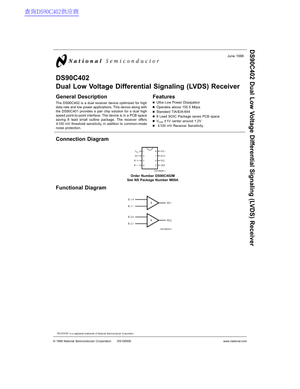
This ultra-low power dual LVDS receiver is optimized for reliable, high data rate point-to-point communication links operating above 155.5 Mbps. Designed in a compact SOIC package, it provides advanced signal reception capabilities using the standard TIA/EIA-644 interface. The comprehensive manual details critical electrical specifications, including differential threshold voltages, propagation delays, skew measurements, and fail-safe termination guidelines. It is essential documentation for engineers developing high-speed embedded systems requiring robust, reliable data signal monitoring.
Page 1 Text Content
查询DS90C402供应商
90C ual Low Voltage ifferential S ignaling (LV eceiver
DS90C402 Dual Low Voltage Differential Signaling (LVDS) Receiver General Description Features
The DS90C402 is dual receiver device optimized for high Ultra Low Power Dissipation
data rate and low power applications. This device along with Operates above 155.5 Mbps the DS90C401 provides pair chip solution for dual high Standard TIA/EIA-644 speed point-to-point interface. The device is in PCB space Lead SOIC Package saves PCB space saving lead small outline package. The receiver offers
VCM ±1V center around 1.2V
±100 m V threshold sensitivity, in addition to common-mode
±100 m V Receiver Sensitivity
noise protection.
Connection Diagram
DS100006-1
Order Number DS90C402M See NS Package Number M08A
Functional Diagram
DS100006-2
TRI-STATE® is registered trademark of National Semiconductor Corporation.
National Semiconductor Corporation DS100006 www.national.com
Page Summary Contents For National DS90C402 Data Sheet
Manual Details
| Brand | National |
|---|---|
| Pages | 8 |
| File Size | 135.35 KB |
| Published | June 01, 2026 |
Enter the captcha to get the download link:

Frequently Asked Questions
How should I properly terminate the connection for this receiver?
A termination resistor of 100Ω must be selected and placed as close to the receiver input pins as possible.
What is the recommended supply voltage range for operation?
The recommended operating input voltage (VIN, VIN-) is between −0.3V and (V + 0.3V), with a supply voltage of 4.5V to 5.5V being optimal.
What happens if I connect voltages outside the specified range?
Input voltages exceeding the defined limits may activate the internal fail-safe ESD protection circuitry.