National DS90C031 Data Sheet
Summary
This professional line driver is a quad CMOS component engineered for ultra low-power differential signal transmission up to 155.5 Mbps. Ideal for engineers developing high-speed, reliable point-to-point data interfaces that require compliance with the standard ANSI/TIA/EIA-644 LVDS protocol and minimal power draw. The technical manual provides comprehensive details on electrical specifications, switching characteristics, absolute maximum ratings, and operational guidelines necessary for successful implementation in complex electronic systems.
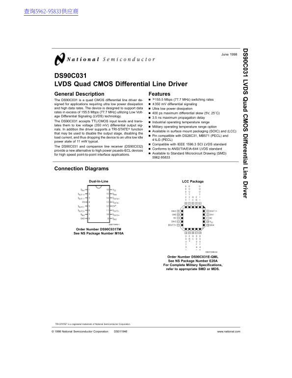
Page 1 Text Content
90C LV uad ifferential Line river
DS90C031 LVDS Quad CMOS Differential Line Driver General Description Features
The DS90C031 is quad CMOS differential line driver de- >155.5 Mbps (77.7 MHz) switching rates signed for applications requiring ultra low power dissipation ±350 m V differential signaling
and high data rates. The device is designed to support data Ultra low power dissipation rates in excess of 155.5 Mbps (77.7 MHz) utilizing Low Volt- ps maximum differential skew (5V, 25˚C) age Differential Signaling (LVDS) technology.
3.5 ns maximum propagation delay
The DS90C031 accepts TTL/CMOS input levels and trans- Industrial operating temperature range lates them to low voltage (350 m V) differential output sig-
Military operating temperature range option
nals. In addition the driver supports TRI-STATE® function
Available in surface mount packaging (SOIC) and (LCC)
that may be used to disable the output stage, disabling the
Pin compatible with DS26C31, MB571 (PECL) and
load current, and thus dropping the device to an ultra low idle
41LG (PECL)
power state of m W typical.
Compatible with IEEE 1596.3 SCI LVDS standard
The DS90C031 and companion line receiver (DS90C032)
Conforms to ANSI/TIA/EIA-644 LVDS standard
provide new alternative to high power psuedo-ECL devices
Available to Standard Microcircuit Drawing (SMD)
for high speed point-to-point interface applications.
Connection Diagrams
Dual-In-Line LCC Package
DS011946-1
Order Number DS90C031TM See NS Package Number M16A
DS011946-33
Order Number DS90C031E-QML See NS Package Number E20A For Complete Military Specifications, refer to appropriate SMD or MDS.
TRI-STATE® is registered trademark of National Semiconductor Corporation.
National Semiconductor Corporation DS011946 www.national.com
Page Summary Contents For National DS90C031 Data Sheet
Manual Details
| Brand | National |
|---|---|
| Pages | 14 |
| File Size | 272.68 KB |
| Published | May 30, 2026 |
Enter the captcha to get the download link:

Frequently Asked Questions
What is the operating temperature range?
The industrial operating temperature range is -40°C to +85°C (for model DS90C031T), while the military version operates from -55°C to +125°C.
Does this device support multiple data standards?
Yes, it accepts TTL/CMOS input levels and is compatible with IEEE 1596.3 SCI LVDS standard.
How low can the output power consumption be when idle?
It can drop to an ultra-low idle power state of 11 mW typical when using the TRI-STATE function.
What are the input and output voltage limits?
The recommended operating supply voltage is +4.5V to +5.5V, with differential output voltage ranges from 345mV to 450mV at R=100Ω.