# A B C D E F G H I J K L M N O P Q R S T U V W X Y Z

National LMX1501A LMX1511 Data Sheet

Summary

The LMX1501A/LMX1511 is a high-performance PLL frequency synthesizer designed for robust RF communications up to 1.1 GHz. Featuring ultra low current consumption and integrated dual modulus prescalers, this component is critical for portable wireless applications, including advanced cellular phone systems and cordless communication networks. This technical manual provides comprehensive information on the device's operation, pin descriptions, electrical characteristics (2.7V–5.5V), and functional block diagrams, ensuring precise integration into demanding wireless hardware designs.
📄 Preview PAGE OF 22

Page 1 Text Content

查询LMX1501供应商

November

tin .1 re

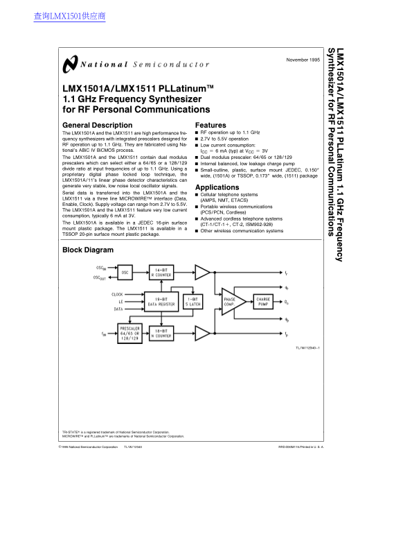
th iz fo rs ic tio LMX1501A/LMX1511 PLLatinum TM 1.1 GHz Frequency Synthesizer for RF Personal Communications General Description Features

The LMX1501A and the LMX1511 are high performance fre- RF operation up to 1.1 GHz

quency synthesizers with integrated prescalers designed for 2.7V to 5.5V operation RF operation up to 1.1 GHz. They are fabricated using Na- Low current consumption: tional’s ABi C IV Bi CMOS process. ICC m A (typ) at VCC 3V The LMX1501A and the LMX1511 contain dual modulus Dual modulus prescaler: 64/65 or 128/129 prescalers which can select either 64/65 or 128/129 Internal balanced, low leakage charge pump divide ratio at input frequencies of up to 1.1 GHz. Using

Small-outline, plastic, surface mount JEDEC, 0.150×

proprietary digital phase locked loop technique, the

wide, (1501A) or TSSOP, 0.173× wide, (1511) package

LMX1501A/11’s linear phase detector characteristics can generate very stable, low noise local oscillator signals.

Applications

Serial data is transferred into the LMX1501A and the

Cellular telephone systems

LMX1511 via three line MICROWIRETM interface (Data,

(AMPS, NMT, ETACS)

Enable, Clock). Supply voltage can range from 2.7V to 5.5V.

Portable wireless communications

The LMX1501A and the LMX1511 feature very low current

(PCS/PCN, Cordless)

consumption, typically m A at 3V.

Advanced cordless telephone systems

The LMX1501A is available in JEDEC 16-pin surface

(CT-1/CT-1a, CT-2, ISM902-928)

mount plastic package. The LMX1511 is available in

Other wireless communication systems

TSSOP 20-pin surface mount plastic package.

Block Diagram

TL/W/12340–1

TRI-STATEÉ is registered trademark of National Semiconductor Corporation. MICROWIRETM and PLLatinum TM are trademarks of National Semiconductor Corporation.

C1995 National Semiconductor Corporation TL/W/12340 RRD-B30M115/Printed in U. S. A.

Page Summary Contents For National LMX1501A LMX1511 Data Sheet

Page 1 查询LMX1501供应商 November tin .1 re th iz fo rs ic tio LMX1501A/LMX1511 PLLatinum TM 1.1 GHz Frequency Synthesizer for RF Personal Communications General Description Features The LMX1501A and the LMX1511 ...
Page 2 Connection Diagrams LMX1501A LMX1511 TL/W/12340–2 JEDEC 16-Lead (0.150× Wide) Small Outline Molded Package (M) TL/W/12340–3 Order Number LMX1501AM or LMX1501AMX 20-Lead (0.173× Wide) Thin Shrink See N...
Page 3 Functional Block Diagram LMX1501A TL/W/12340–40
Page 4 Functional Block Diagram (Continued) LMX1511 TL/W/12340–4
Page 5 Absolute Maximum Ratings (Note 1) Recommended Operating If Military/Aerospace specified devices are required, Conditions please contact the National Semiconductor Sales Power Supply Voltage Office/Dis...
Page 6 Electrical Characteristics VCC 5.0V, VP 5.0V; b40§C TA 85§C, except as specified (Continued) Symbol Parameter Conditions Min Typ Max Units IDo-source Charge Pump Output Current VDo VP/2 b5.0 m A IDo-s...
Page 7 Typical Performance Characteristics ICC vs VCC IDo TRI-STATE vs Do Voltage TL/W/12340–5 TL/W/12340–6 Charge Pump Current vs Do Voltage Charge Pump Current vs Do Voltage TL/W/12340–7 TL/W/12340–8 Charg...
Page 8 Typical Performance Characteristics (Continued) Input Sensitivity vs Frequency Input Sensitivity vs Frequency TL/W/12340–11 TL/W/12340–12 Input Sensitivity at Temperature Input Sensitivity at Temperat...
Page 9 Charge Pump Current Specification Definitions TL/W/12340–17 I1 CP sink current at VDo VP DV I4 CP source current at VDo VP DV I2 CP sink current at VDo VP/2 I5 CP source current at VDo VP/2 I3 CP sink...
Page 10 Functional Description The simplified block diagram below shows the 19-bit data register, the 14-bit Counter and the Latch, and the 18-bit Counter (intermediate latches are not shown). The data stream...
Page 11 Functional Description (Continued) PROGRAMMABLE DIVIDER (N COUNTER) The counter consists of the 7-bit swallow counter (A counter) and the 11-bit programmable counter (B counter). If the Control Bit (l...
Page 12 Functional Description (Continued) SERIAL DATA INPUT TIMING TL/W/12340–22 Notes: Parenthesis data indicates programmable reference divider data. Data shifted into register on clock rising edge. Data i...
Page 13 Analog Switch (1511 only) The analog switch is useful for radio systems that utilize frequency scanning mode and narrow band mode. The purpose of the analog switch is to decrease the loop filter time ...
Page 14 Typical Application Example TL/W/12340–28 Operational Notes: *VCO is assumed AC coupled. **RIN increases impedance so that VCO output power is provided to the load rather than the PLL. Typical values ...
Page 15 Application Information LOOP FILTER DESIGN block diagram of the basic phase locked loop is shown. TL/W/12340–30 FIGURE 1. Basic Charge Pump Phase Locked Loop An example of passive loop filter configur...
Page 16 Application Information (Continued) Therefore, if we specify the loop bandwidth, 0p, and the In choosing the loop filter components trade off must be phase margin, wp, Equations through allow us to ca...
Page 17 Application Information (Continued) Example Ý1 KVCO 19.3 MHz/V Kw m A (Note 1) RFopt MHz Fref k Hz RFopt/fref 0p 2q k Hz 3.1415e4 wp 43§ ATTEN d B secwp tanwp T1 1.38eb5 T3 9.361eb6 010(10/20) (2q 25e...
Page 18 Application Information (Continued) TL/W/12340–43 TL/W/12340–45 FIGURE 5. PLL Reference Spurs FIGURE 6. PLL Phase Noise 3.5 k Hz Offset The reference spurious level is b66 d Bc, due to the loop The ph...
Page 19 Application Information (Continued) EXTERNAL CHARGE PUMP EXAMPLE The LMX PLLatimum series of frequency synthesizers are Typical Device Parameters bn e100, bp equipped with an internal balanced charge ...
Page 21 Physical Dimensions inches (millimeters) JEDEC 16-Lead (0.150× Wide) Small Outline Molded Package (M) Order Number LMX1501AM For Tape and Reel Order Number LMX1501AMX (2500 Units per Reel) NS Package ...
Page 22 ti .1 re th iz fo rs ic ti Physical Dimensions (millimeters) (Continued) 20-Lead (0.173× Wide) Thin Shrink Small Outline Package (TM) Order Number LMX1511TM For Tape and Reel Order Number LMX1511TMX (...

Manual Details

Brand National
Pages 22
File Size 370.23 KB
Published June 04, 2026
49 views

Enter the captcha to get the download link:

captcha

Frequently Asked Questions

What is the recommended operating power supply voltage?

The power supply voltage (VCC) should operate between 2.7V and 5.5V.

What frequency range does this synthesizer support?

It provides RF operation up to 1.1 GHz.

How low is the current consumption?

The typical low current consumption is 6 mA at Vcc of 3V.

What are the package options for these ICs?

LMX1501A comes in a JEDEC 16-pin TSSOP, and LMX1511 uses a 20-pin TSSOP.