National LMH6642EP LMH6643EP LMH6644EP Data Sheet
Summary
These low power, high-speed amplifiers are designed for demanding industrial and commercial signal processing applications. The series offers exceptional rail-to-rail output capabilities at a single supply voltage, ensuring wide dynamic range and maintaining integrity even under varying load conditions. This comprehensive manual provides detailed specifications on key performance metrics, covering 130MHz operation, low distortion, fast slew rates, and robust stability across various temperature and power demands, making them ideal for ADC buffers and high-frequency filters.
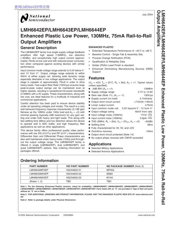
Page 1 Text Content
查询LMH6643EP供应商 LM 6642E /LM 6643E /LM 6644E nhanced lastic Low ow er,130M z,75m ail-to-R ail
utput plifiers
LMH6642EP/LMH6643EP/LMH6644EP Enhanced Plastic Low Power, 130MHz, 75m A Rail-to-Rail Output Amplifiers
ENHANCED PLASTIC
General Description
Extended Temperature Performance of −40˚C to +85˚C
The LMH664XEP family true single supply voltage feedback
Baseline Control Single Fab Assembly Site
amplifiers offer high speed (130MHz), low distortion
(−62d Bc), and exceptionally high output current (approxi- Process Change Notification (PCN)
mately 75m A) at low cost and with reduced power consump-
Qualification Reliability Data
tion when compared against existing devices with similar
Solder (Pb Sn) Lead Finish is standard
performance.
Enhanced Diminishing Manufacturing Sources (DMS)
Input common mode voltage range extends to 0.5V below V−
Support
and 1V from V+. Output voltage range extends to within 40m V of either supply rail, allowing wide dynamic range
Features
especially desirable in low voltage applications. The output stage is capable of approximately 75m A in order to drive (VS ±5V, TA 25˚C, RL 2kΩ, AV +1. Typical values heavy loads. Fast output Slew Rate (130V/µs) ensures large unless specified). peak-to-peak output swings can be maintained even at
−3d B BW (AV +1) 130MHz
higher speeds, resulting in exceptional full power bandwidth
Supply voltage range 2.7V to 12.8V
of 40MHz with 3V supply. These characteristics, along with
Slew rate (Note 11), (AV −1) 130V/µs
low cost, are ideal features for multitude of industrial and
Supply current (no load) 2.7m A/amp
commercial applications.
Output short circuit current +115m A/−145m A
Careful attention has been paid to ensure device stability
Linear output current ±75m A
under all operating voltages and modes. The result is very
Input common mode volt. 0.5V beyond V−, 1V from V+
well behaved frequency response characteristic (0.1d B gain
flatness up the 12MHz under 150Ω load and AV +2) with Output voltage swing 40m V from rails minimal peaking (typically 2d B maximum) for any gain set- Input voltage noise (100k Hz) 17n V/
ting and under both heavy and light loads. This along with Input current noise (100k Hz) 0.9p A/ fast settling time (68ns) and low distortion allows the device THD (5MHz, RL 2kΩ, VO 2VPP, AV +2) −62d Bc to operate well in ADC buffer, and high frequency filter
Settling time 68ns
applications as well as other applications.
Fully characterized for 3V, 5V, and ±5V
This device family offers professional quality video perfor-
Overdrive recovery 100ns
mance with low DG (0.01%) and DP (0.01˚) characteristics.
Output short circuit protected (Note 14)
Differential Gain and Differential Phase characteristics are
No output phase reversal with CMVR exceeded
also well maintained under heavy loads (150Ω) and through- out the output voltage range. The LMH664XEP family is
offered in single (LMH6642EP), dual (LMH6643EP), and Applications
quad (LMH6644EP) options. See ordering information for Selected Military Applications packages offered. Selected Avionics Applications
Ordering Information PART NUMBER VID PART NUMBER NS PACKAGE NUMBER (Note 3) LMH6642MFXEP V62/04625-01 MF05A LMH6643MAXEP V62/04625-02 M08A LMH6644MAXEP V62/04625-03 M14A (Notes 1, 2) TBD TBD
Note 1: For the following (Enhanced Plastic) versions, check for availability: LMH6642MAEP, LMH6642MAXEP, LMH6642MFEP, LMH6643MAEP, LMH6643MMEP, LMH6643MMXEP, LMH6644MAEP, LMH6644MTEP, LMH6644MTXEP. Parts listed with an "X" are provided in Tape Reel and parts without an "X" are in Rails. Note 2: FOR ADDITIONAL ORDERING AND PRODUCT INFORMATION, PLEASE VISIT THE ENHANCED PLASTIC WEB SITE AT: www.national.com/ mil Note 3: Refer to package details under Physical Dimensions
National Semiconductor Corporation DS200894 www.national.com
Page Summary Contents For National LMH6642EP LMH6643EP LMH6644EP Data Sheet
Manual Details
| Brand | National |
|---|---|
| Pages | 21 |
| File Size | 945.78 KB |
| Published | June 01, 2026 |
Enter the captcha to get the download link:

Frequently Asked Questions
What is the operational temperature range for this amplifier family?
It offers an extended operating temperature performance of −40˚C to +85˚C.
Does this product line support various channel configurations?
Yes, it is available in single (LMH6642EP), dual (LMH6643EP), and quad (LMH6644EP) options.
What is the acceptable supply voltage range for use with the amplifier?
The device supports a stable single supply voltage range from 2.7V to 12.8V.
How close to the power rails can the output swing reach?
The output voltage range extends extremely wide, reaching within 40mV of either supply rail.