National DAC1020/1021/1022 Data Sheet
Summary
High-precision Digital-to-Analog Converters (DACs) designed for critical signal processing applications. This manual provides comprehensive details on the DAC10xx and DAC12xx series, covering technical specifications, linearity accuracy, low power consumption, and robust operation across various logic levels (TTL/CMOS). Ideal for engineers developing advanced measurement or control systems requiring stable voltage conversion resolution.
Page 1 Text Content
查询AD7521JD供应商
-B it in ry ltip ly in rte
-B it in ry ltip ly in rte
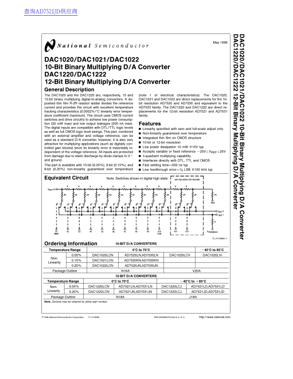
DAC1020/DAC1021/DAC1022 10-Bit Binary Multiplying D/A Converter DAC1220/DAC1222 12-Bit Binary Multiplying D/A Converter General Description
The DAC1020 and the DAC1220 are, respectively, and (note of electrical characteristics). The DAC1020, 12-bit binary multiplying digital-to-analog converters. de- DAC1021 and DAC1022 are direct replacements for the 10- posited thin film R-2R resistor ladder divides the reference bit resolution AD7520 and AD7530 and equivalent to the current and provides the circuit with excellent temperature AD7533 family. The DAC1220 and DAC1222 are direct re- tracking characteristics (0.0002%/§C linearity error temper- placements for the 12-bit resolution AD7521 and AD7531 ature coefficient maximum). The circuit uses CMOS current family.
switches and drive circuitry to achieve low power consump- tion (30 m W max) and low output leakages (200 n A max). Features The digital inputs are compatible with DTL/TTL logic levels
Linearity specified with zero and full-scale adjust only
as well as full CMOS logic level swings. This part, combined
Non-linearity guaranteed over temperature
with an external amplifier and voltage reference, can be
Integrated thin film on CMOS structure
used as standard D/A converter; however, it is also very
10-bit or 12-bit resolution
attractive for multiplying applications (such as digitally con-
Low power dissipation m W @15V typ
trolled gain blocks) since its linearity error is essentially in-
dependent of the voltage reference. All inputs are protected Accepts variable or fixed reference b25Vs VREFs25V
from damage due to static discharge by diode clamps to Va 4-quadrant multiplying capability and ground. Interfaces directly with DTL, TTL and CMOS This part is available with 10-bit (0.05%), 9-bit (0.10%), and Fast settling timeÐ500 ns typ
8-bit (0.20%) non-linearity guaranteed over temperature Low feedthrough errorÐ(/2 LSB @100 k Hz typ
Equivalent Circuit Note. Switches shown in digital high state
TL/H/5689–1
Information 10-BIT D/A CONVERTERSOrdering
Temperature Range 0§C to 70§C b40§C to 85§C
0.05% DAC1020LCN AD7520LN,AD7530LN DAC1020LCV DAC1020LIV
0.10% DAC1021LCN AD7520KN,AD7530KN
Linearity
0.20% DAC1022LCN AD7520JN,AD7530JN
Package Outline N16A V20A
12-BIT D/A CONVERTERS
Temperature Range 0§C to 70§C b40§C to a85§C
Non- 0.05% DAC1220LCN AD7521LN,AD7531LN DAC1220LCJ AD7521LD,AD7531LD
Linearity 0.20% DAC1222LCN AD7521JN,AD7531JN DAC1222LCJ AD7521JD,AD7531JD
Package Outline N18A J18A Note. Devices may be ordered by either part number.
C1996 National Semiconductor Corporation TL/H/5689 RRD-B30M96/Printed in U. S. A. http://www.national.com
Page Summary Contents For National DAC1020/1021/1022 Data Sheet
Manual Details
| Brand | National |
|---|---|
| Pages | 14 |
| File Size | 266.64 KB |
| Published | June 04, 2026 |
Enter the captcha to get the download link:

Frequently Asked Questions
What logic levels can the digital inputs support?
The digital inputs are compatible with DTL, TTL, and CMOS logic levels.
How accurate is the linearity of the converter?
For 10-bit parts like DAC1020/DAC1220, the minimum typical linearity error is listed as 0.05%.
What is the expected power dissipation and leakage?
The circuit uses CMOS technology to achieve low power consumption (e.g., max 30 mW) and low output leakages (200 nA max).
Are these converters suitable for multiplying applications?
Yes, they are attractive for multiplying applications due to their ability to provide 4-quadrant multiplying capability.