MAXIM MAX4674 Wideband Quad 2 1 Analog Multiplexer Datasheet
Summary
The MAX4674 is a low-voltage CMOS analog switch featuring four 2:1 multiplexers, ideal for high-performance signal routing. This manual provides comprehensive technical details, including electrical specifications, absolute maximum ratings, and single-supply operation capabilities from +1.8V to +5.5V. It is designed for engineers implementing complex data acquisition systems, base-T communication links, or video/audio signal processing where robust isolation and compatibility with TTL/CMOS logic are essential.
Page 1 Text Content
19-1708; Rev 3; 12/06
3V/5V, 4Ω, Wideband Quad 2:1 Analog Multiplexer
General Description Features
The MAX4674 is a low-voltage CMOS analog switch con- Guaranteed On-Resistance taining four 2:1 multiplexers/demultiplexer. When pow- 4Ω max (+5V Supply) ered from a single +5V supply, it features a low 4Ω max 6Ω max (+3V Supply) on-resistance (RON), 0.4Ω max RON matching between Guaranteed Match Between Channels channels, and 0.8Ω RON flatness over the entire signal 0.4Ω max range. Off-leakage current is only 0.5n A max at +25°C.
Guaranteed Flatness Over Signal Range
The MAX4674 features fast turn-on (t ON) and turn-off 0.8Ω max (t OFF) times of 18ns and 6ns, respectively, and is avail- 1.8V Operation able in QFN, QSOP, TSSOP, and SO packages. RON = 100Ω typ Over Temperature
This low-voltage multiplexer operates with a +1.8V to t ON = 51ns typ +5.5V single supply. All digital inputs have +0.8V and t OFF = 13ns typ
+2.4V logic thresholds, ensuring TTL/CMOS-logic com- Guaranteed Low Leakage Currents patibility with +5V operation. 0.5n A max at +25°C
Single-Supply Operation from +1.8V to +5.5V
________________________Applications
Rail-to-Rail Signal Handling
10/100 Base-T
TTL/CMOS-Logic Compatible
ATM Switching Crosstalk: -114d B (1MHz)
Audio and Video Signal Routing Off-Isolation: -67d B (1MHz) 4mm ✕ 4mm QFN Package
Low-Voltage Data-Acquisition Systems Communications Circuits
Ordering Information
Relay Replacement
PIN - PK G
PA R T T EM P
R A N G E PA C K A G E C O D E
M AX 4674E E E - 40°C to + 85° C 16 QS OP E 16- 4 M AX 4674E U E - 40°C to + 85° C 16 TS S O P U 16- 2 M AX 4674E S E - 40°C to + 85° C 16 N ar r ow S O S 16- 2 M AX 4674E GE - 40°C to + 85° C 16 QFN - E P * G 1644- 1
M AX 4674E GP - 40°C to + 85° C 20 QFN - E P * G 2044- 3
*EP = Exposed pad.
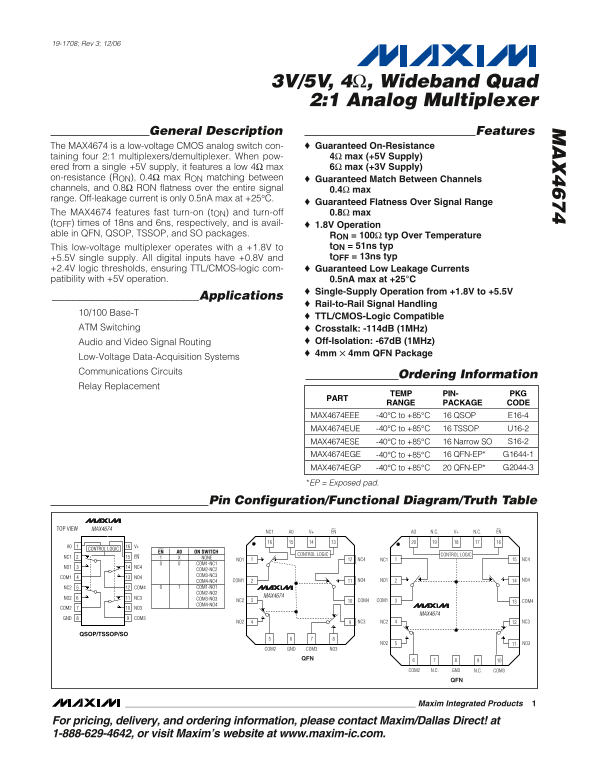
Pin Configuration/Functional Diagram/Truth Table
TOP VIEW MAX4674
NC1 A0 V+ EN AO N.C. V+ N.C. EN
CONTROL LOGIC
EN A0 ON SWITCH
CONTROL LOGIC CONTROL LOGIC
NC1 EN NONE
NO1 NC4 NC1 NC4
COM1-NC1
NO1 NC4
COM2-NC2 COM3-NC3
COM1 NO4
COM4-NC4 COM1 NO4 NO1 NO4
NC2 COM4 COM1-NO1 COM2-NO2
MAX4674
NO2 NC3 COM3-NO3
NC2 COM4 3COM1 COM4
COM4-NO4
COM2 NO3
MAX4674
GND COM3
NO2 NC3 NC2 NC3
QSOP/TSSOP/SO
NO2 NO3
COM2 NO3COM3GND
COM2 GND COM3N.C.N.C.
Maxim Integrated Products
For pricing, delivery, and ordering information, please contact Maxim/Dallas Direct! at 1-888-629-4642, or visit Maxim’s website at www.maxim-ic.com.
Page Summary Contents For MAXIM MAX4674 Wideband Quad 2 1 Analog Multiplexer Datasheet
Manual Details
| Brand | QUAD |
|---|---|
| Pages | 13 |
| File Size | 596.10 KB |
| Published | June 04, 2026 |
Enter the captcha to get the download link:

Frequently Asked Questions
What is the guaranteed on-resistance match between channels?
With a +5V supply, the guaranteed channel matching of the On-Resistance ($R_{ON}$) is 0.4 Ohm max.
What operating temperature range does this device support?
The MAX4674E operates within a temperature range from -40°C to +85°C.
Can I use this multiplexer with TTL/CMOS logic?
Yes, the digital inputs have dedicated thresholds at +0.8V and +2.4V, ensuring compatibility with TTL/CMOS logic.