LINEAR Triple Output DC-DC µModule® Regulator in 15mm x 15mm x 2.8mm SMT Package Replaces Up to 30 Discrete Components Design Note 469
Summary
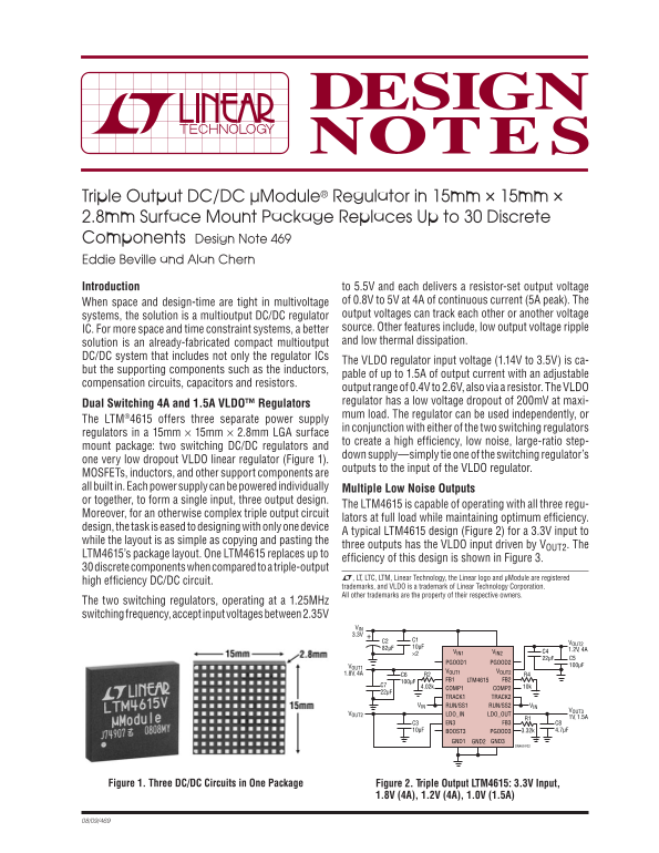
This Design Note 469 from Linear Technology presents the LTM4615 triple-output DC/DC micro-module regulator housed in a 15 mm by 15 mm by 2.8 mm LGA surface-mount package that replaces up to 30 discrete components with built-in MOSFETs, inductors, and support components. The device integrates two switching DC/DC regulators each delivering 4 A continuous at 5 A peak with adjustable outputs from 0.8 V to 5 V from a 2.375 V to 5.5 V input, plus a VLDO linear regulator capable of 1.5 A output with a
Page 1 Text Content
Triple Output DC/DC µModule® Regulator in 15mm × 15mm × 2.8mm Surface Mount Package Replaces Up to 30 Discrete Components Design Note 469 Eddie Beville and Alan Chern Introduction to 5.5V and each delivers a resistor-set output voltage
When space and design-time are tight in multivoltage of 0.8V to 5V at 4A of continuous current (5A peak). The systems, the solution is a multioutput DC/DC regulator output voltages can track each other or another voltage IC. For more space and time constraint systems, a better source. Other features include, low output voltage ripple solution is an already-fabricated compact multioutput and low thermal dissipation.
DC/DC system that includes not only the regulator ICs
The VLDO regulator input voltage (1.14V to 3.5V) is ca-
but the supporting components such as the inductors,
pable of up to 1.5A of output current with an adjustable
compensation circuits, capacitors and resistors.
output range of 0.4V to 2.6V, also via a resistor. The VLDO Dual Switching 4A and 1.5A VLDO™ Regulators regulator has a low voltage dropout of 200m V at maxi- mum load. The regulator can be used independently, or
The LTM®4615 offers three separate power supply
in conjunction with either of the two switching regulators
regulators in a 15mm × 15mm × 2.8mm LGA surface
to create a high effi ciency, low noise, large-ratio step-
mount package: two switching DC/DC regulators and
down supply—simply tie one of the switching regulator’s
one very low dropout VLDO linear regulator (Figure 1).
outputs to the input of the VLDO regulator.
MOSFETs, inductors, and other support components are all built in. Each power supply can be powered individually Multiple Low Noise Outputs or together, to form a single input, three output design.
The LTM4615 is capable of operating with all three regu-
Moreover, for an otherwise complex triple output circuit
lators at full load while maintaining optimum effi ciency.
design, the task is eased to designing with only one device
A typical LTM4615 design (Figure 2) for a 3.3V input to
while the layout is as simple as copying and pasting the
three outputs has the VLDO input driven by VOUT2. The
LTM4615’s package layout. One LTM4615 replaces up to
effi ciency of this design is shown in Figure 3.
30 discrete components when compared to a triple-output
L, LT, LTC, LTM, Linear Technology, the Linear logo and μModule are registered
high effi ciency DC/DC circuit.
trademarks, and VLDO is a trademark of Linear Technology Corporation. All other trademarks are the property of their respective owners.
The two switching regulators, operating at a 1.25MHz switching frequency, accept input voltages between 2.35V
VIN 3.3V
VOUT2
VIN1 VIN2
PGOOD1 PGOOD2
VOUT1 100μF
VOUT1 VOUT2
100μF FB1 LTM4615 FB2
COMP1 COMP2
TRACK1 TRACK2
VIN RUN/SS1 RUN/SS2 VIN
VOUT3
VOUT2 LDO_IN LDO_OUT
C3 EN3 FB3 C8
10μF BOOST3 PGOOD3 3.32k 4.7μF
GND1 GND2 GND3
DN469 F02
Figure 1. Three DC/DC Circuits in One Package Figure 2. Triple Output LTM4615: 3.3V Input,
Page Summary Contents For LINEAR Triple Output DC-DC µModule® Regulator in 15mm x 15mm x 2.8mm SMT Package Replaces Up to 30 Discrete Components Design Note 469
Manual Details
| Brand | Linear |
|---|---|
| Pages | 2 |
| File Size | 127.22 KB |
| Published | June 18, 2026 |
Enter the captcha to get the download link:
