LINEAR LT1130A, LT1140A Series Data Handbook
Summary
Discover the LT1130A/LT1140A series, advanced low power RS232 drivers/receivers designed for high-integrity communication systems. Featuring superior ESD protection and bipolar robustness, these transceivers ensure reliable data transfer up to 250kbaud. This technical guide provides engineers with comprehensive specifications, usage guidelines, and detailed application examples for integrating robust, industry-leading serial connectivity into their electronic designs.
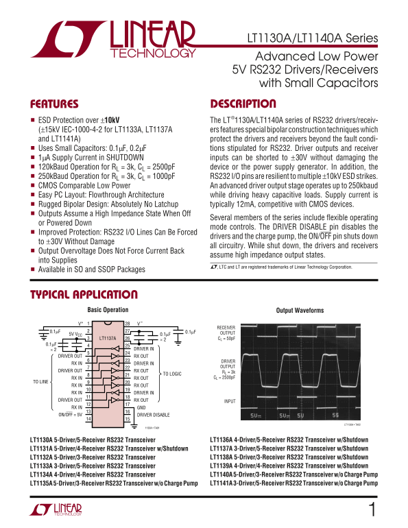
Page 1 Text Content
LT1130A/LT1140A Series Advanced Low Power 5V RS232 Drivers/Receivers with Small Capacitors FEATURES DESCRIPTIO
ESD Protection over ±10k V The LT®1130A/LT1140A series of RS232 drivers/receiv- (±15k V IEC-1000-4-2 for LT1133A, LT1137A ers features special bipolar construction techniques which and LT1141A) protect the drivers and receivers beyond the fault condi- Uses Small Capacitors: 0.1µF, 0.2µF tions stipulated for RS232. Driver outputs and receiver
1µA Supply Current in SHUTDOWN inputs can be shorted to ±30V without damaging the 120k Baud Operation for RL = 3k, CL = 2500p F device or the power supply generator. In addition, the 250k Baud Operation for RL = 3k, CL = 1000p F RS232 I/O pins are resilient to multiple ±10k V ESD strikes. CMOS Comparable Low Power An advanced driver output stage operates up to 250kbaud Easy PC Layout: Flowthrough Architecture while driving heavy capacitive loads. Supply current is Rugged Bipolar Design: Absolutely No Latchup typically 12m A, competitive with CMOS devices.
Outputs Assume a High Impedance State When Off
Several members of the series include flexible operating
or Powered Down
mode controls. The DRIVER DISABLE pin disables the
Improved Protection: RS232 I/O Lines Can Be Forced
drivers and the charge pump, the ON/OFF pin shuts down
to ±30V Without Damage
all circuitry. While shut down, the drivers and receivers
Output Overvoltage Does Not Force Current Back
assume high impedance output states.
into Supplies
, LTC and LT are registered trademarks of Linear Technology Corporation.
Available in SO and SSOP Packages
TYPICAL APPLICATIO
Basic Operation Output Waveforms
RECEIVER
5V VCC 0.1µF OUTPUT
LT1137A × 2 CL = 50p F
× 2 DRIVER IN
DRIVER OUT RX OUT
DRIVER
RX IN DRIVER IN
OUTPUT
DRIVER OUT RX OUT RL = 3k
TO LOGIC
RX IN RX OUT CL = 2500p F
TO LINE
RX IN RX OUT RX IN DRIVER IN DRIVER OUT RX OUT INPUT RX IN GND ON/OFF = 5V DRIVER DISABLE
LT1130A • TA02
1130A • TA01
LT1130A 5-Driver/5-Receiver RS232 Transceiver LT1136A 4-Driver/5-Receiver RS232 Transceiver w/Shutdown LT1131A 5-Driver/4-Receiver RS232 Transceiver w/Shutdown LT1137A 3-Driver/5-Receiver RS232 Transceiver w/Shutdown LT1132A 5-Driver/3-Receiver RS232 Transceiver LT1138A 5-Driver/3-Receiver RS232 Transceiver w/Shutdown LT1133A 3-Driver/5-Receiver RS232 Transceiver LT1139A 4-Driver/4-Receiver RS232 Transceiver w/Shutdown LT1134A 4-Driver/4-Receiver RS232 Transceiver LT1140A 5-Driver/3-Receiver RS232 Transceiver w/o Charge Pump LT1135A 5-Driver/3-Receiver RS232 Transceiver w/o Charge Pump LT1141A 3-Driver/5-Receiver RS232 Transceiver w/o Charge Pump
Page Summary Contents For LINEAR LT1130A, LT1140A Series Data Handbook
Manual Details
| Brand | Linear |
|---|---|
| Pages | 13 |
| File Size | 204.94 KB |
| Published | June 21, 2026 |
Enter the captcha to get the download link:

Frequently Asked Questions
What is the maximum baud rate supported by the driver output stage?
The advanced driver output stage operates up to 250kbaud.
How is the device protected against electrical surges?
It features nESD protection over –10kV, and the RS232 I/O lines are resilient to multiple ESD strikes.
When power is removed via the ON/OFF pin, what happens to the outputs?
The drivers and receivers assume a high impedance output state when shut down to –30V, which does not force current back into the supplies.
What is the minimum short-circuit tolerance time for the device's voltage levels?
The series supports up to a 30-second duration short circuit at specified operating voltages.