LINEAR dn399f Data Manual
Summary
Optimize your optical signal conditioning with advanced low noise photodiode amplifiers. This manual provides detailed engineering guidelines and design comparisons for high-performance transimpedance circuits used with both small and large area photodiodes. Learn how to mitigate input capacitance effects, manage current versus voltage noise sources, and implement circuit enhancements—such as JFET bootstrapping—to maximize signal integrity, bandwidth, and sensitivity in professional measurement equipment.
Page 1 Text Content
advertisement
Low Noise Amplifi ers for Small and Large Area Photodiodes Design Note 399 Glen Brisebois
Introduction
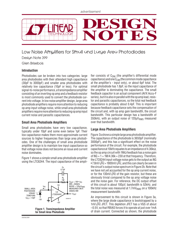
Photodiodes can be broken into two categories: large fi er consists of CDM (the amplifi er’s differential mode area photodiodes with their attendant high capacitance capacitance) and one CCM (the common mode capacitance (30p F to 3000p F) and smaller area photodiodes with at the amplifi er’s - input only), or about 6p F total. The relatively low capacitance (10p F or less). For optimal small photodiode has 1.8p F, so the input capacitance of signal-to-noise performance, a transimpedance amplifi er the amplifi er is dominating the capacitance. The small consisting of an inverting op amp and a feedback resistor feedback capacitor is an actual component (AVX Accu-F is most commonly used to convert the photodiode cur- series), but it is also in parallel with the op amp lead, resis- rent into voltage. In low noise amplifi er design, large area tor and parasitic capacitances, so the total real feedback photodiode amplifi ers require more attention to reducing capacitance is probably about 0.4p F. This is important op amp input voltage noise, while small area photodiode because feedback capacitance sets the compensation of amplifi ers require more attention to reducing op amp input the circuit and, with op amp gain bandwidth, the circuit current noise and parasitic capacitances. bandwidth. This particular design has a bandwidth of 350k Hz, with an output noise of 120µVRMS measured Small Area Photodiode Amplifi ers over that bandwidth.
Small area photodiodes have very low capacitance,
Large Area Photodiode Amplifi ers
typically under 10p F and some even below 1p F. Their
low capacitance makes them more approximate current Figure 2a shows a simple large area photodiode amplifi er. sources to higher frequencies than large area photodi- The capacitance of the photodiode is 3650p F (nominally odes. One of the challenges of small area photodiode 3000p F), and this has a signifi cant effect on the noise amplifi er design is to maintain low input capacitance so performance of the circuit. For example, the photodiode that voltage noise does not become an issue and current capacitance at 10k Hz equates to an impedance of 4.36kΩ, noise dominates. so the op amp circuit with 1MΩ feedback has a noise gain of NG = 1 + 1M/4.36k = 230 at that frequency. Therefore,
Figure 1 shows a simple small area photodiode amplifi er
the LTC6244 input voltage noise gets to the output as NG
using the LTC6244. The input capacitance of the ampli-
• 7.8n V/√Hz = 1800n V/√Hz, and this can clearly be seen in CF the circuit’s output noise spectrum in Figure 2b. Note that
we have not yet accounted for the op amp current noise, or for the 130n V/√Hz of the gain resistor, but these are
RF obviously trivial compared to the op amp voltage noise 1M
VOUT = 1M • IPD and the noise gain. For reference, the DC output offset
BW = 350k Hz
5V of this circuit is about 100µV, bandwidth is 52k Hz, and
IPD NOISE = 120µVRMS
SMALL AREA MEASURED ON A the total noise was measured at 1.7m VRMS on a 100k Hz
PHOTODIODE 350k Hz BW
1/2 measurement bandwidth.
VISHAY VOUT
LTC6244HV
TEMD1000
CPD = 1.8p F An improvement to this circuit is shown in Figure 3a,
DN399 FO1
where the large diode capacitance is bootstrapped by a
1n V/√Hz JFET. This depletion JFET has a VGS of about –0.5V, so that RBIAS forces it to operate at just over 1m A
Figure 1. Transimpedance Amplifi er
of drain current. Connected as shown, the photodiode
for Small Area Photodiode
Page Summary Contents For LINEAR dn399f Data Manual
Manual Details
| Brand | Linear |
|---|---|
| Pages | 2 |
| File Size | 96.04 KB |
| Published | June 20, 2026 |
Enter the captcha to get the download link:

Frequently Asked Questions
How does using a JFET bootstrap affect the circuit's performance and noise?
The JFET bootstrap significantly improves both noise and bandwidth compared to the previous design, drastically reducing the output noise.
What are the primary factors determining small area photodiode amplifier noise?
In low noise amp design for small photodiodes, current noise and parasitic capacitances are the main concerns.
Is high photovoltaic capacitance a concern with large-area photodiodes?
Yes, the capacitance of large photodiodes (like 3650pF) has a significant effect on noise, particularly in transimpedance amplifiers.