Intel Intersil ACTS541MS Radiation-Hardened Octal Three-State Buffer Line Driver Data Sheet
Summary
The ACTS541MS is an octa buffer/line driver engineered with advanced Radiation Hardened SOS CMOS technology for critical electronics. This component provides high reliability, featuring excellent immunity to Single Event Upsets (SEU) and extreme temperature operation (-55°C to +125°C). The technical manual details its usage, providing comprehensive pinouts, electrical specifications, functional diagrams, and military-grade qualifications (MIL-PRF-38535). It is ideal for engineers designing robust systems requiring reliable data transmission in demanding, radiation-exposed environments.
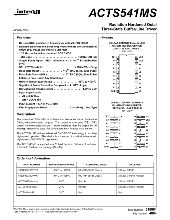
Page 1 Text Content
ACTS541MS Radiation Hardened Octal January 1996 Three-State Buffer/Line Driver
Features Pinouts
Devices QML Qualified in Accordance with MIL-PRF-38535 20 LEAD CERAMIC DUAL-IN-LINE MIL-STD-1835 DESIGNATOR,
Detailed Electrical and Screening Requirements are Contained in
CDIP2-T20, LEAD FINISH C
SMD# 5962-96726 and Intersil’s QM Plan
TOP VIEW
1.25 Micron Radiation Hardened SOS CMOS
Total Dose . . . . . . . . . . . . . . . . . . . . . . . . . . . . . . . . >300K RAD (Si) 1OE1 VCC Single Event Upset (SEU) Immunity: <1 x 10⁻¹⁰ Errors/Bit/Day A0 OE2
(Typ)
SEU LET Threshold . . . . . . . . . . . . . . . . . . . . . . . >100 MEV-cm2/mg
Dose Rate Upset . . . . . . . . . . . . . . . . >1011 RAD (Si)/s, 20ns Pulse
Dose Rate Survivability . . . . . . . . . . . >1012 RAD (Si)/s, 20ns Pulse
Latch-Up Free Under Any Conditions
Military Temperature Range . . . . . . . . . . . . . . . . . . -55o C to +125o C
Significant Power Reduction Compared to ALSTTL Logic
DC Operating Voltage Range . . . . . . . . . . . . . . . . . . . . 4.5V to 5.5V
GND Y7
Input Logic Levels VIL = 0.8V Max VIH = VCC/2 Min
20 LEAD CERAMIC FLATPACK
Input Current ≤ 1µA at VOL, VOH
MIL-STD-1835 DESIGNATOR,
Fast Propagation Delay . . . . . . . . . . . . . . . . 21ns (Max), 14ns (Typ) CDFP4-F20, LEAD FINISH C
TOP VIEW
Description
OE1 VCC
The Intersil ACTS541MS is a Radiation Hardened Octal Buffer/Line A0 OE2 Driver, with three-state outputs. The output enable pins OE1, OE2 Y0
control the three-state outputs. If either enable is high the output will be
in a high impedance state. For data output both enables must be low.
A3 Y2 The ACTS541MS utilizes advanced CMOS/SOS technology to achieve A4 Y3
high-speed operation. This device is a member of a radiation hardened, A5 Y4 high-speed, CMOS/SOS Logic family. A6 Y5
The ACTS541MS is supplied in a 20 lead Ceramic Flatpack (K suffix) or
GND Y7
a Ceramic Dual-In-Line package (D suffix).
Ordering Information PART NUMBER TEMPERATURE RANGE SCREENING LEVEL PACKAGE
5962F9672601VRC -55o C to +125o C MIL-PRF-38535 Class V 20 Lead SBDIP
5962F9672601VXC -55o C to +125o C MIL-PRF-38535 Class V 20 Lead Ceramic Flatpack
ACTS541D/Sample 25o C Sample 20 Lead SBDIP
ACTS541K/Sample 25o C Sample 20 Lead Ceramic Flatpack
ACTS541HMSR 25o C Die Die
CAUTION: These devices are sensitive to electrostatic discharge; follow proper IC Handling Procedures.
Spec Number
1-888-INTERSIL or 321-724-7143 Copyright © Intersil Corporation 1999
File Number
Page Summary Contents For Intel Intersil ACTS541MS Radiation-Hardened Octal Three-State Buffer Line Driver Data Sheet
Manual Details
| Brand | Intel |
|---|---|
| Pages | 3 |
| File Size | 66.48 KB |
| Published | May 30, 2026 |
Enter the captcha to get the download link:

Frequently Asked Questions
What temperature range can this component operate in?
The military operating temperature range is -55°C to +125°C.
How must I configure the enable pins for data output?
For the outputs (Y0 through Y6) to provide data, both enable pins (OE1 and OE2) must be set to a low logic level.
What is the usable operating voltage window (VCC)?
The DC Operating Voltage Range is specified as 4.5V to 5.5V.
Are there any specific safety precautions when handling this device?
Yes, these devices are sensitive to electrostatic discharge; proper IC Handling Procedures must be followed.