Fairchild RMBA19500A Data Handbook
Summary
A high-linearity Power Amplifier designed for demanding wireless infrastructure, this component is ideal for PCS1900 base stations or as the output stage in Micro- and Pico-Cell environments. This manual serves as a comprehensive guide for RF engineers, providing critical electrical specifications, absolute ratings, operational guidelines, and detailed functional block diagrams. It ensures proper system integration by detailing required external bias circuits and matching networks needed to achieve peak performance at the 1930–1990 MHz frequency range.
Page 1 Text Content
查询RMBA19500A供应商
May 2004
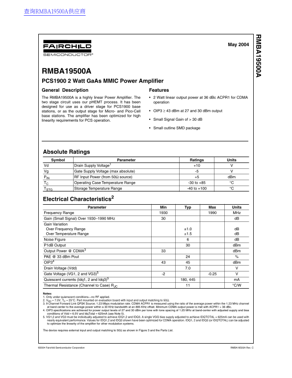
RMBA19500A PCS1900 2 Watt Ga As MMIC Power Amplifier General Description Features The RMBA19500A is a highly linear Power Amplifier. The 2 Watt linear output power at 36 d Bc ACPR1 for CDMA two stage circuit uses our p HEMT process. It has been operation designed for use as a driver stage for PCS1900 base
stations, or as the output stage for Micro- and Pico-Cell OIP3 43 d Bm at 27 and 30 d Bm output
base stations. The amplifier has been optimized for high
linearity requirements for PCS operation. Small Signal Gain of > 30 d B
Small outline SMD package
Absolute Ratings Symbol Parameter Ratings Units Vd Drain Supply Voltage +10 Vg Gate Supply Voltage (max absolute) -5
RF Input Power (from 50 source) +5 d Bm
Operating Case Temperature Range -30 to +85 °C Storage Temperature Range -40 to +100 °C
Electrical Characteristics
Parameter Min Typ Max Units
Frequency Range MHz Gain (Small Signal) Over 1930–1990 MHz d B Gain Variation Over Frequency Range ±1.0 d B Over Temperature Range ±1.5 d B Noise Figure d B P1d B Output d Bm Output Power @ CDMA d Bm PAE @ 33 d Bm Pout OIP3 d Bm Drain Voltage (Vdd) 7.0 Gate Voltage (VG1, 2 and VG3) -2 -0.25
Quiescent currents (Idq1, 2 and Idq3) 180, 445 m A
Thermal Resistance (Channel to Case) R °C/W
Notes: 1. Only under quienscent conditions—no RF applied. 2. V DD = 7.0V, T = 25°C. Part mounted on evaluation board with input and output matching to 50 3. 9 Channel Forward Link QPSK Source; 1.23 Mbps modulation rate. CDMA ACPR1 is measured using the ratio of the average power within the 1.23 MHz channel at band center to the average power within a 30 KHz bandwidth at an 885 KHz offset. Minimum CDMA output power is met with ACPR1 > 36 d Bc. 4. OIP3 specifications are achieved for power output levels of 27 and 30 d Bm per tone with tone spacing of 1.25 MHz at band-center with adjusted supply and bias conditions of Vdd = 6.5V and Idq Total = 625m A (see Note 5). 5. VG1,2 and VG3 must be individually adjusted to achieve IDQ1,2 and IDQ3. A single VGG bias supply adjusted to achieve IDQTOTAL = 625m A can be used with nearly equivalent performance. Values for IDQ1,2 and IDQ3 shown have been optimized for CDMA operation. IDQ1, 2 and IDQ3 (or IDQTOTAL) can be adjusted to optimize the linearity of the amplifier for other modulation systems.
The device requires external input and output matching to 50 as shown in Figure 3 and the Parts List.
©2004 Fairchild Semiconductor Corporation RMBA19500A Rev. C
Page Summary Contents For Fairchild RMBA19500A Data Handbook
Manual Details
| Brand | Fairchild |
|---|---|
| Pages | 7 |
| File Size | 79.68 KB |
| Published | June 20, 2026 |
Enter the captcha to get the download link:

Frequently Asked Questions
What is required besides the device itself?
External passive components are needed for DC bias and RF input/output matching circuits.
Does this unit need special mounting?
Yes, the base of the package must be soldered onto a heat sink for proper operation.
Is this component safe to handle during setup?
Caution: This is an ESD sensitive device and requires careful handling.
What power systems can the RMBA19500A support?
It is designed for use with PCS1900, Micro-, or Pico-Cell base stations.