Fairchild Power Factor Correction Converter Design with FAN6982 User Guide
Summary
Discover detailed insights on the FAN6982, a robust Power Factor Correction (PFC) controller IC designed for high-efficiency power supplies. This technical guide provides comprehensive coverage of the device's operation theory, including boost converter modes, current/voltage control loops, and advanced features like line feed-forward and brownout protection. Ideal for electrical engineers and product developers building regulated DC/DC converters requiring reliable PFC functionality in demanding high-power applications.
Page 1 Text Content
www.fairchildsemi.com
AN-6982 Power Factor Correction Converter Design with FAN6982
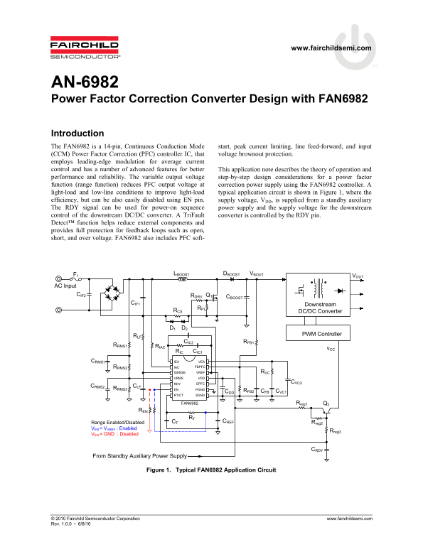
Introduction The FAN6982 is a 14-pin, Continuous Conduction Mode start, peak current limiting, line feed-forward, and input (CCM) Power Factor Correction (PFC) controller IC, that voltage brownout protection. employs leading-edge modulation for average current control and has a number of advanced features for better This application note describes the theory of operation and performance and reliability. The variable output voltage step-by-step design considerations for a power factor function (range function) reduces PFC output voltage at correction power supply using the FAN6982 controller. A light-load and low-line conditions to improve light-load typical application circuit is shown in Figure 1, where the efficiency, but can be also easily disabled using EN pin. supply voltage, VDD, is supplied from a standby auxiliary The RDY signal can be used for power-on sequence power supply and the supply voltage for the downstream control of the downstream DC/DC converter. A Tri Fault converter is controlled by the RDY pin. Detect™ function helps reduce external components and provides full protection for feedback loops such as open, short, and over voltage. FAN6982 also includes PFC soft-
F1 LBOOST DBOOST VBOUT
AC Input CIF2 RDRV Q1
CBOOST
Downstream
RCS DC/DC Converter
PWM Controller
CIC2 RFB1
RRMS1 RIAC
RIC CIC1
CRMS1 IEA VEA
RRMS2 IAC FBPFC
ISENSE VREF RVC
VRMS VDD
OPFC CVC2
CRMS2 CLF
RRMS3 EN PGND
CDD RFB2 CFB CVC1
RT/CT SGND
FAN6982 Q2Rreg1
Range Enabled/Disabled CREF Rreg2
VEN VVREF : Enabled
Rreg3
VEN GND : Disabled
From Standby Auxiliary Power Supply
Figure 1. Typical FAN6982 Application Circuit
© 2010 Fairchild Semiconductor Corporation www.fairchildsemi.com Rev. 1.0.0 • 6/8/10
Page Summary Contents For Fairchild Power Factor Correction Converter Design with FAN6982 User Guide
Manual Details
| Brand | Fairchild |
|---|---|
| Pages | 15 |
| File Size | 676.42 KB |
| Published | June 01, 2026 |
Enter the captcha to get the download link:

Frequently Asked Questions
What kind of power correction does the FAN6982 controller provide?
It is a Power Factor Correction (PFC) controller that operates in Continuous Conduction Mode (CCM).
How can I maintain PFC efficiency during light loads?
The advanced features, such as those shown in Figure 1, are designed to maintain high efficiency even under light-load and low-line conditions.
What is the purpose of the EN pin on the FAN6982?
The EN pin allows the entire PFC function to be easily disabled when not needed.
How does line feed-forward improve performance?
It uses line voltage information for generating a reference, which helps maintain optimal operation and accuracy for power factors.