Fairchild PCB Grounding System and FAN2001 - High Performance DC-DC Converters Data Manual
Summary
Optimize your hardware design with this essential guide to high-performance PCB grounding systems. This application note details sophisticated star grounding techniques necessary for integrating complex DC-DC converters and sensitive linear circuits. Learn how proper ground plane management minimizes system noise, reduces circulating currents, and eliminates voltage offsets caused by parasitic resistance. Ideal for electrical engineers and circuit designers developing demanding electronic equipment like communication devices or power supplies who require maximum signal fidelity and stable operation.
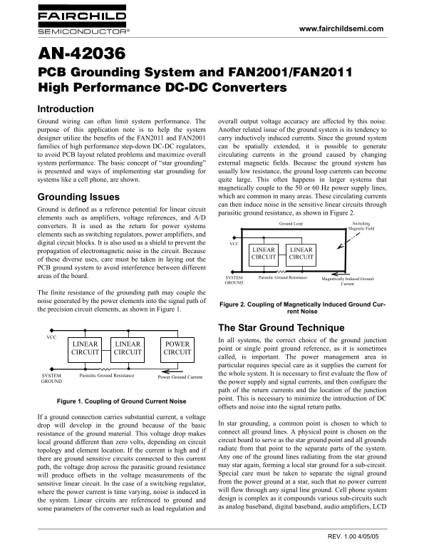
Page 1 Text Content
www.fairchildsemi.com
AN-42036 PCB Grounding System and FAN2001/FAN2011 High Performance DC-DC Converters Introduction
Ground wiring can often limit system performance. The overall output voltage accuracy are affected by this noise. purpose of this application note is to help the system Another related issue of the ground system is its tendency to designer utilize the benefits of the FAN2011 and FAN2001 carry inductively induced currents. Since the ground system families of high performance step-down DC-DC regulators, can be spatially extended, it is possible to generate to avoid PCB layout related problems and maximize overall circulating currents in the ground caused by changing system performance. The basic concept of “star grounding” external magnetic fields. Because the ground system has is presented and ways of implementing star grounding for usually low resistance, the ground loop currents can become systems like a cell phone, are shown. quite large. This often happens in larger systems that magnetically couple to the 50 or 60 Hz power supply lines, Grounding Issues which are common in many areas. These circulating currents can then induce noise in the sensitive linear circuits through
Ground is defined as a reference potential for linear circuit
parasitic ground resistance, as shown in Figure 2.
elements such as amplifiers, voltage references, and A/D
Ground Loop Switching
converters. It is used as the return for power systems
Magnetic Field
elements such as switching regulators, power amplifiers, and digital circuit blocks. It is also used as a shield to prevent the VCC
propagation of electromagnetic noise in the circuit. Because LINEAR LINEAR CIRCUIT CIRCUIT
of these diverse uses, care must be taken in laying out the PCB ground system to avoid interference between different areas of the board. SYSTEM Parasitic Ground Resistance Magnetically Induced Ground
GROUND Current
The finite resistance of the grounding path may couple the noise generated by the power elements into the signal path of
Figure 2. Coupling of Magnetically Induced Ground Cur-
the precision circuit elements, as shown in Figure 1.
rent Noise
The Star Ground Technique
In all systems, the correct choice of the ground junction
LINEAR LINEAR POWER
point or single point ground reference, as it is sometimes
CIRCUIT CIRCUIT CIRCUIT
called, is important. The power management area in particular requires special care as it supplies the current for Parasitic Ground Resistance Power Ground Current SYSTEM the whole system. It is necessary to first evaluate the flow of
GROUND the power supply and signal currents, and then configure the
path of the return currents and the location of the junction point. This is necessary to minimize the introduction of DC
Figure 1. Coupling of Ground Current Noise
offsets and noise into the signal return paths.
If a ground connection carries substantial current, a voltage
In star grounding, a common point is chosen to which to
drop will develop in the ground because of the basic
connect all ground lines. A physical point is chosen on the
resistance of the ground material. This voltage drop makes
circuit board to serve as the star ground point and all grounds
local ground different than zero volts, depending on circuit
radiate from that point to the separate parts of the system.
topology and element location. If the current is high and if
Any one of the ground lines radiating from the star ground
there are ground sensitive circuits connected to this current
may star again, forming a local star ground for a sub-circuit.
path, the voltage drop across the parasitic ground resistance
Special care must be taken to separate the signal ground
will produce offsets in the voltage measurements of the
from the power ground at a star, such that no power current
sensitive linear circuit. In the case of a switching regulator,
will flow through any signal line ground. Cell phone system
where the power current is time varying, noise is induced in
design is complex as it compounds various sub-circuits such
the system. Linear circuits are referenced to ground and
as analog baseband, digital baseband, audio amplifiers, LCD
some parameters of the converter such as load regulation and
REV. 1.00 4/05/05
Page Summary Contents For Fairchild PCB Grounding System and FAN2001 - High Performance DC-DC Converters Data Manual
Manual Details
| Brand | Fairchild |
|---|---|
| Pages | 3 |
| File Size | 143.49 KB |
| Published | June 05, 2026 |
Enter the captcha to get the download link:

Frequently Asked Questions
What effect can poor grounding have on my system's performance?
Ground wiring resistance can couple noise, affecting the overall output voltage accuracy and potentially causing instability in linear circuits.
What is the primary benefit of using the 'star ground' technique?
It helps eliminate ground noise problems caused by substantial parasitic resistance within Printed Circuit Board traces.
How should I approach PCB layout when implementing a complex ground system?
First, evaluate the flow of power supply and signal currents; then configure the return current paths and the location of the junction point to minimize DC offsets.
Is it safe to connect all grounds together in a large system?
Connecting all grounds can create voltage drops due to parasitic resistance, requiring special caution to separate sensitive linear circuits from high-current power paths.