Fairchild NM34W02 Data Handbook
Summary
The NM34W02 is a reliable, 2K-bit serial EEPROM memory specifically engineered for Serial Presence Detect (SPD) applications in PC100 compliant modules. It provides non-volatile data storage with robust features like full array write protection and low power consumption options (L/LZ). This manual offers comprehensive technical details, including the I²C communication protocol, detailed electrical specifications, thermal ratings, and multiple package types. It is ideal for memory controllers, microprocessor designers, and embedded systems requiring reliable identification and management of PC main memory modules.
Page 1 Text Content
34W 02 2K -B it S tan ard 2-W ire B s In terface S erial E ith ll A rray W rite P ro tect
March 1999
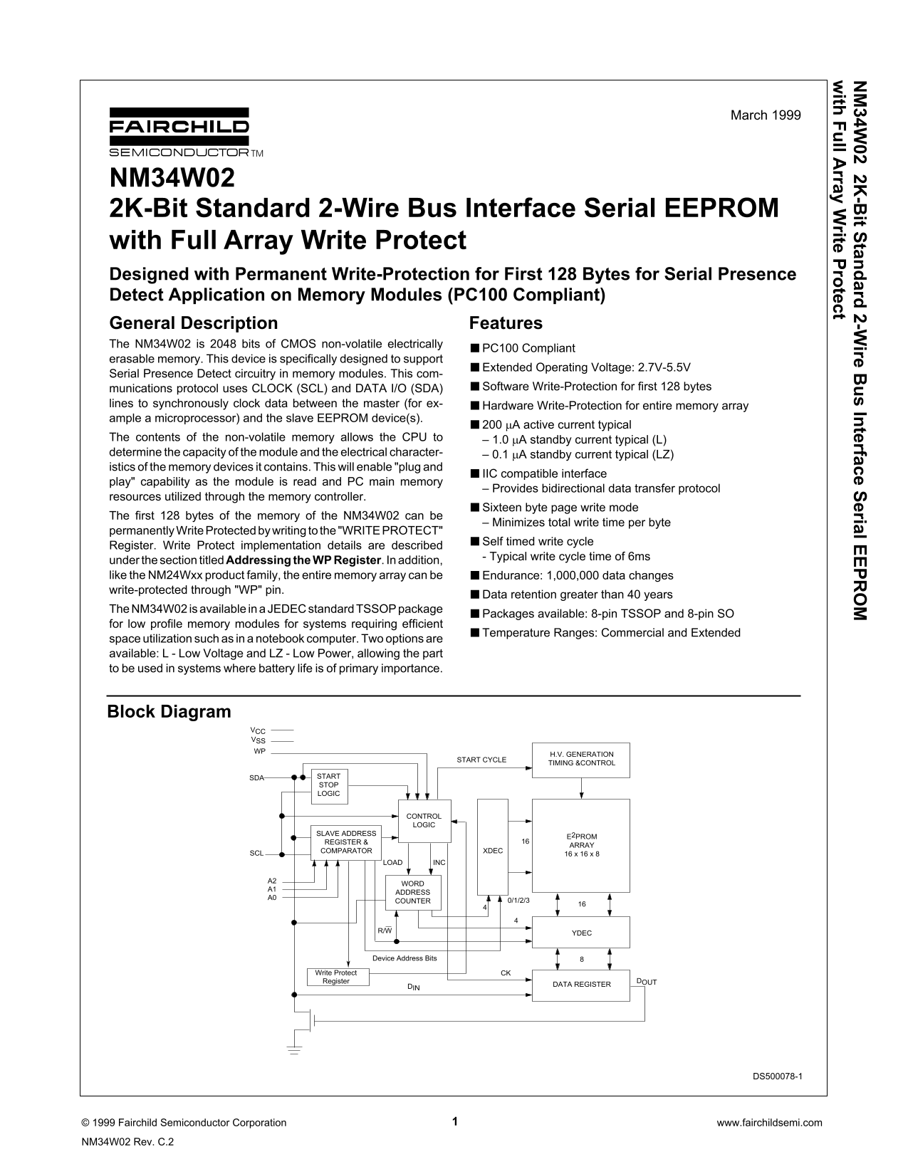
NM34W02 2K-Bit Standard 2-Wire Bus Interface Serial EEPROM with Full Array Write Protect Designed with Permanent Write-Protection for First 128 Bytes for Serial Presence Detect Application on Memory Modules (PC100 Compliant) General Description Features The NM34W02 is 2048 bits of CMOS non-volatile electrically
PC100 Compliant
erasable memory. This device is specifically designed to support
Extended Operating Voltage: 2.7V-5.5V
Serial Presence Detect circuitry in memory modules. This com-
munications protocol uses CLOCK (SCL) and DATA I/O (SDA) Software Write-Protection for first 128 bytes
lines to synchronously clock data between the master (for ex- Hardware Write-Protection for entire memory array ample a microprocessor) and the slave EEPROM device(s).
200 µA active current typical
The contents of the non-volatile memory allows the CPU to – 1.0 µA standby current typical (L) determine the capacity of the module and the electrical character- – 0.1 µA standby current typical (LZ) istics of the memory devices it contains. This will enable "plug and
IIC compatible interface
play" capability as the module is read and PC main memory
– Provides bidirectional data transfer protocol
resources utilized through the memory controller.
Sixteen byte page write mode
The first 128 bytes of the memory of the NM34W02 can be
– Minimizes total write time per byte
permanently Write Protected by writing to the "WRITE PROTECT"
Self timed write cycle
Register. Write Protect implementation details are described
- Typical write cycle time of 6ms
under the section titled Addressing the WP Register. In addition, like the NM24Wxx product family, the entire memory array can be Endurance: 1,000,000 data changes write-protected through "WP" pin.
Data retention greater than 40 years
The NM34W02 is available in a JEDEC standard TSSOP package
Packages available: 8-pin TSSOP and 8-pin SO
for low profile memory modules for systems requiring efficient
Temperature Ranges: Commercial and Extended
space utilization such as in a notebook computer. Two options are available: L - Low Voltage and LZ - Low Power, allowing the part to be used in systems where battery life is of primary importance.
Block Diagram
VCC VSS WP
H.V. GENERATION
START CYCLE
TIMING &CONTROL
SDA START STOP LOGIC
CONTROL LOGIC
SLAVE ADDRESS
E2PROM
REGISTER &
ARRAY
SCL COMPARATOR XDEC
LOAD INC
A2 WORD A1
ADDRESS
COUNTER
R/W YDEC
Device Address Bits
Write Protect CK
Register DOUT
DIN DATA REGISTER
DS500078-1
© 1999 Fairchild Semiconductor Corporation www.fairchildsemi.com NM34W02 Rev. C.2
Page Summary Contents For Fairchild NM34W02 Data Handbook
Manual Details
| Brand | Fairchild |
|---|---|
| Pages | 12 |
| File Size | 93.08 KB |
| Published | July 06, 2026 |
Enter the captcha to get the download link:

Frequently Asked Questions
What interface lines does the EEPROM use for communication?
It utilizes CLOCK (SCL) and DATA I/O (SDA) lines to communicate between master and slave devices.
Does this memory have permanent write protection features?
Yes, it includes hardware write-protection for the first 128 bytes, in addition to full array write-protect capability via the 'WP' pin.
What is the expected lifetime or endurance of the memory?
The device offers high durability with an endurance rating of 1,000,000 data changes and data retention greater than 40 years.
Can this component be used in low power systems?
Yes, it provides Low Voltage (L) and Low Power (LZ) options, allowing operation down to 2.7V in battery-sensitive applications.