Fairchild NC7WZ00 Data Handbook
Summary
The NC7WZ00 is a high-speed, space-saving dual 2-Input NAND Gate designed for sophisticated digital circuit design. Featuring an advanced CMOS structure and US8 surface mount package, this logic gate delivers ultra-high operational speed (t < 2.4ns) and reliable performance across a broad 1.65V to 5.5V operating range. This comprehensive manual provides detailed technical specifications, absolute maximum ratings, electrical characteristics, and recommended conditions, making it an essential resource for electronics engineers building advanced embedded systems or high-performance digital logic that requires overvoltage tolerance and minimal power dissipation.
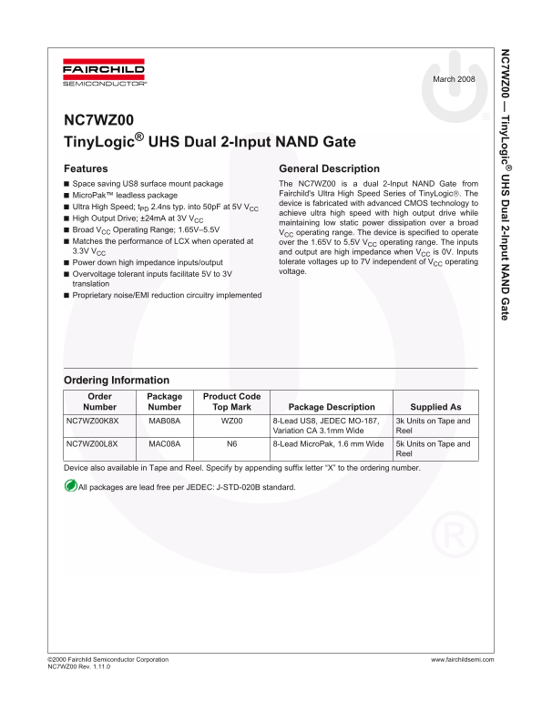
Page 1 Text Content
7W 00 — iny L ic al 2-In t N ate
March 2008
NC7WZ00 Tiny Logic® UHS Dual 2-Input NAND Gate Features General Description Space saving US8 surface mount package The NC7WZ00 is a dual 2-Input NAND Gate from
Micro Pak™ leadless package Fairchild's Ultra High Speed Series of Tiny Logic. The device is fabricated with advanced CMOS technology to
Ultra High Speed; t PD 2.4ns typ. into 50p F at 5V VCC
achieve ultra high speed with high output drive while
High Output Drive; ±24m A at 3V VCC
maintaining low static power dissipation over a broad
Broad VCC Operating Range; 1.65V–5.5V
VCC operating range. The device is specified to operate
Matches the performance of LCX when operated at over the 1.65V to 5.5V VCC operating range. The inputs 3.3V VCC and output are high impedance when VCC is 0V. Inputs
Power down high impedance inputs/output tolerate voltages up to 7V independent of VCC operating voltage.
Overvoltage tolerant inputs facilitate 5V to 3V translation Proprietary noise/EMI reduction circuitry implemented
Ordering Information Order Package Product Code Number Number Top Mark Package Description Supplied As NC7WZ00K8X MAB08A WZ00 8-Lead US8, JEDEC MO-187, 3k Units on Tape and
Variation CA 3.1mm Wide Reel
NC7WZ00L8X MAC08A N6 8-Lead Micro Pak, 1.6 mm Wide 5k Units on Tape and
Device also available in Tape and Reel. Specify by appending suffix letter “X” to the ordering number.
All packages are lead free per JEDEC: J-STD-020B standard.
©2 000 Fairchild Semiconductor Corporation www.fairchildsemi.com NC 7WZ00 Rev. 1.11.0
Page Summary Contents For Fairchild NC7WZ00 Data Handbook
Manual Details
| Brand | Fairchild |
|---|---|
| Pages | 10 |
| File Size | 651.29 KB |
| Published | June 05, 2026 |
Enter the captcha to get the download link:

Frequently Asked Questions
What is the typical propagation delay for this NAND gate?
The typical propagation delay (t) is 2.4ns into 50pF at 5V V PD CC.
What is the recommended operating voltage range?
The device should operate within a Supply Voltage range of 1.65V to 5.5V, and input/output voltages from 0V to 5.5V.
Are unused inputs allowed to float when powering down?
No; all unused inputs must be held either HIGH or LOW. They may not float.
What is the maximum safe operating temperature range?
The recommended operating temperature range (T Operating) is from –40°C to +85°C.